SNVS179F February 2003 – September 2015 LP3995
PRODUCTION DATA.
- 1 Features
- 2 Applications
- 3 Description
- 4 Revision History
- 5 Pin Configuration and Functions
- 6 Specifications
- 7 Parameter Measurement Information
- 8 Detailed Description
- 9 Application and Implementation
- 10Power Supply Recommendations
- 11Layout
- 12Device and Documentation Support
- 13Mechanical, Packaging, and Orderable Information
9 Application and Implementation
NOTE
Information in the following applications sections is not part of the TI component specification, and TI does not warrant its accuracy or completeness. TI’s customers are responsible for determining suitability of components for their purposes. Customers should validate and test their design implementation to confirm system functionality.
9.1 Application Information
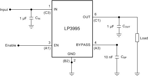
The LP3995 can provide 150-mA output current with 2.5-V to 6-V input. It is stable with a 1-μF ceramic output capacitor. An optional external bypass capacitor reduces the output noise without slowing down the load transient response. Typical output noise is 25 μVRMS at frequencies from 10 Hz to 100 kHz. Typical power supply rejection is 60 dB at 1 kHz.
9.2 Typical Application
 Figure 18. LP3995 Typical Application
9.2.1 Design Requirements
For typical CMOS voltage regulator applications, use the parameters listed in Table 1.
Table 1. Design Parameters
| DESIGN PARAMETER | EXAMPLE VALUE |
|---|---|
| Minimum input voltage | 2.5 V |
| Minimum output voltage | 1.8 V |
| Output current | 150 mA |
9.2.2 Detailed Design Procedure
9.2.2.1 External Capacitors
In common with most regulators, the LP3995 requires external capacitors to ensure stable operation. The LP3995 is specifically designed for portable applications requiring minimum board space and smallest components. These capacitors must be correctly selected for good performance.
9.2.2.2 Input Capacitor
An input capacitor is required for stability. It is recommended that a 1-µF capacitor be connected between the LP3995 IN pin and ground (this capacitance value may be increased without limit).
This capacitor must be located a distance of not more than 1 cm from the IN pin and returned to a clean analogue ground. Any good quality ceramic, tantalum, or film capacitor may be used at the input.
NOTE
Tantalum capacitors can suffer catastrophic failures due to surge current when connected to a low-impedance source of power (like a battery or a very large capacitor). If a tantalum capacitor is used at the input, it must be ensured by the manufacturer to have a surge current rating sufficient for the application.
There are no requirements for the equivalent series resistance (ESR) on the input capacitor, but tolerance and temperature coefficient must be considered when selecting the capacitor to ensure the capacitance remains ≅ 1 µF over the entire operating temperature range.
9.2.2.3 Output Capacitor
The LP3995 is designed specifically to work with very small ceramic output capacitors. A ceramic capacitor (dielectric types Z5U, Y5V or X7R) in the 1-µF to 10-µF range, and with ESR between 5 mΩ to 500 mΩ, is suitable in the LP3995 application circuit.
For this device the output capacitor should be connected between the OUT pin and ground.
It may also be possible to use tantalum or film capacitors at the device output, VOUT, but these are not as attractive for reasons of size and cost (see Capacitor Characteristics).
The output capacitor must meet the requirement for the minimum value of capacitance and also have an ESR value that is within the range 5 mΩ to 500 mΩ for stability.
Table 2. Recommended Output Capacitor
| PARAMETER | TEST CONDITIONS | MIN | TYP | MAX | Units | |
|---|---|---|---|---|---|---|
| COUT | Output Capacitor | Capacitance(1) | 0.7 | 1 | µF | |
| ESR | 5 | 500 | mΩ | |||
9.2.2.4 No-Load Stability
The LP3995 remains stable and in regulation with no external load. This is an important consideration in some circuits, for example CMOS RAM keep-alive applications.
9.2.2.5 Capacitor Characteristics
The LP3995 is designed to work with ceramic capacitors on the output to take advantage of the benefits they offer. For capacitance values in the range of 1 µF to 4.7 µF, ceramic capacitors are the smallest, least expensive and have the lowest ESR values, thus making them best for eliminating high frequency noise. The ESR of a typical 1-µF ceramic capacitor is in the range of 20 mΩ to 40 mΩ, which easily meets the ESR requirement for stability for the LP3995.
The temperature performance of ceramic capacitors varies by type. Most large value ceramic capacitors (≥ 2.2 µF) are manufactured with Z5U or Y5V temperature characteristics, which results in the capacitance dropping by more than 50% as the temperature goes from 25°C to +85°C.
A better choice for temperature coefficient in a ceramic capacitor is X7R. This type of capacitor is the most stable and holds the capacitance within ±15% over the temperature range. Tantalum capacitors are less desirable than ceramic for use as output capacitors because they are more expensive when comparing equivalent capacitance and voltage ratings in the 1-µF to 4.7-µF range.
Another important consideration is that tantalum capacitors have higher ESR values than equivalent size ceramics. This means that while it may be possible to find a tantalum capacitor with an ESR value within the stable range, it would have to be larger in capacitance (which means bigger and more costly) than a ceramic capacitor with the same ESR value. It should also be noted that the ESR of a typical tantalum increases about 2:1 as the temperature goes from 25°C down to −40°C, so some guard band must be allowed.
9.2.2.6 Noise Bypass Capacitor
A bypass capacitor should be connected between the BYPASS pin and ground to significantly reduce the noise at the regulator output. This device pin connects directly to a high impedance node within the bandgap reference circuitry. Any significant loading on this node causes a change on the regulated output voltage. For this reason, DC leakage current through this pin must be kept as low as possible for best output voltage accuracy.
The use of a 0.01-µF bypass capacitor is strongly recommended to prevent overshoot on the output during start-up.
The types of capacitors best suited for the noise bypass capacitor are ceramic and film. High quality ceramic capacitors with NPO or COG dielectric typically have very low leakage. Polypropolene and polycarbonate film capacitors are available in small surface-mount packages and typically have extremely low leakage current.
Unlike many other LDOs, the addition of a noise reduction capacitor does not effect the transient response of the device.
9.2.2.7 Fast Turnoff and Turnon
The controlled switch-off feature of the device provides a fast turn off by discharging the output capacitor via an internal FET device. This discharge is current limited by the RDSon of this switch. Fast turnon is ensured by control circuitry within the reference block allowing a very fast ramp of the output voltage to reach the target voltage.
9.2.2.8 Power Dissipation
The permissible power dissipation for any package is a measure of the capability of the device to pass heat from the power source, the junctions of the device, to the ultimate heat sink, the ambient environment. Thus the power dissipation is dependent on the ambient temperature and the thermal resistance across the various interfaces between the die and ambient air.
Equation 1 restates the equation given in note 5 of Absolute Maximum Ratings:
The allowable power dissipation for the device in a given package can be calculated:
With an RθJA = 255°C/W, the device in the DSBGA package returns a value of 392 mW with a maximum junction temperature of 125°C.
With an RθJA = 88°C/W, the device in the WSON package returns a value of 1.136 mW with a maximum junction temperature of 125°C.
The actual power dissipation across the device can be represented by Equation 3:
This establishes the relationship between the power dissipation allowed due to thermal consideration, the voltage drop across the device, and the continuous current capability of the device. Equation 2 and Equation 3 should be used to determine the optimum operating conditions for the device in the application.
This thermal resistance (RθJA) is highly dependent on the heat-spreading capability of the particular PCB design, and therefore varies according to the total copper area, copper weight, and location of the planes. The RθJA recorded in Thermal Information is determined by the specific EIA/JEDEC JESD51-7 standard for PCB and copper-spreading area and is to be used only as a relative measure of package thermal performance. For a well-designed thermal layout, RθJA is actually the sum of the package junction-to-case (bottom) thermal resistance (RθJCbot) plus the thermal resistance contribution by the PCB copper area acting as a heatsink.
9.2.2.9 Estimating Junction Temperature
The EIA/JEDEC standard recommends the use of psi (Ψ) thermal characteristics to estimate the junction temperatures of surface mount devices on a typical PCB board application. These characteristics are not true thermal resistance values, but rather package specific thermal characteristics that offer practical and relative means of estimating junction temperatures. These psi metrics are determined to be significantly independent of copper-spreading area. The key thermal characteristics (ΨJT and ΨJB) are given in Thermal Information and are used in accordance with Equation 4 or Equation 5.
where
- PD(MAX) is explained in Equation 2
- TTOP is the temperature measured at the center-top of the device package.
where
- PD(MAX) is explained in Equation 2.
- TBOARD is the PCB surface temperature measured 1-mm from the device package and centered on the package edge.
For more information about the thermal characteristics ΨJT and ΨJB, see TI Application Report Semiconductor and IC Package Thermal Metrics (SPRA953); for more information about measuring TTOP and TBOARD, see the TI Application Report Using New Thermal Metrics (SBVA025); and for more information about the EIA/JEDEC JESD51 PCB used for validating RθJA, see the TI Application Report Thermal Characteristics of Linear and Logic Packages Using JEDEC PCB Designs (SZZA017). Aforementioned application notes are available at www.ti.com.
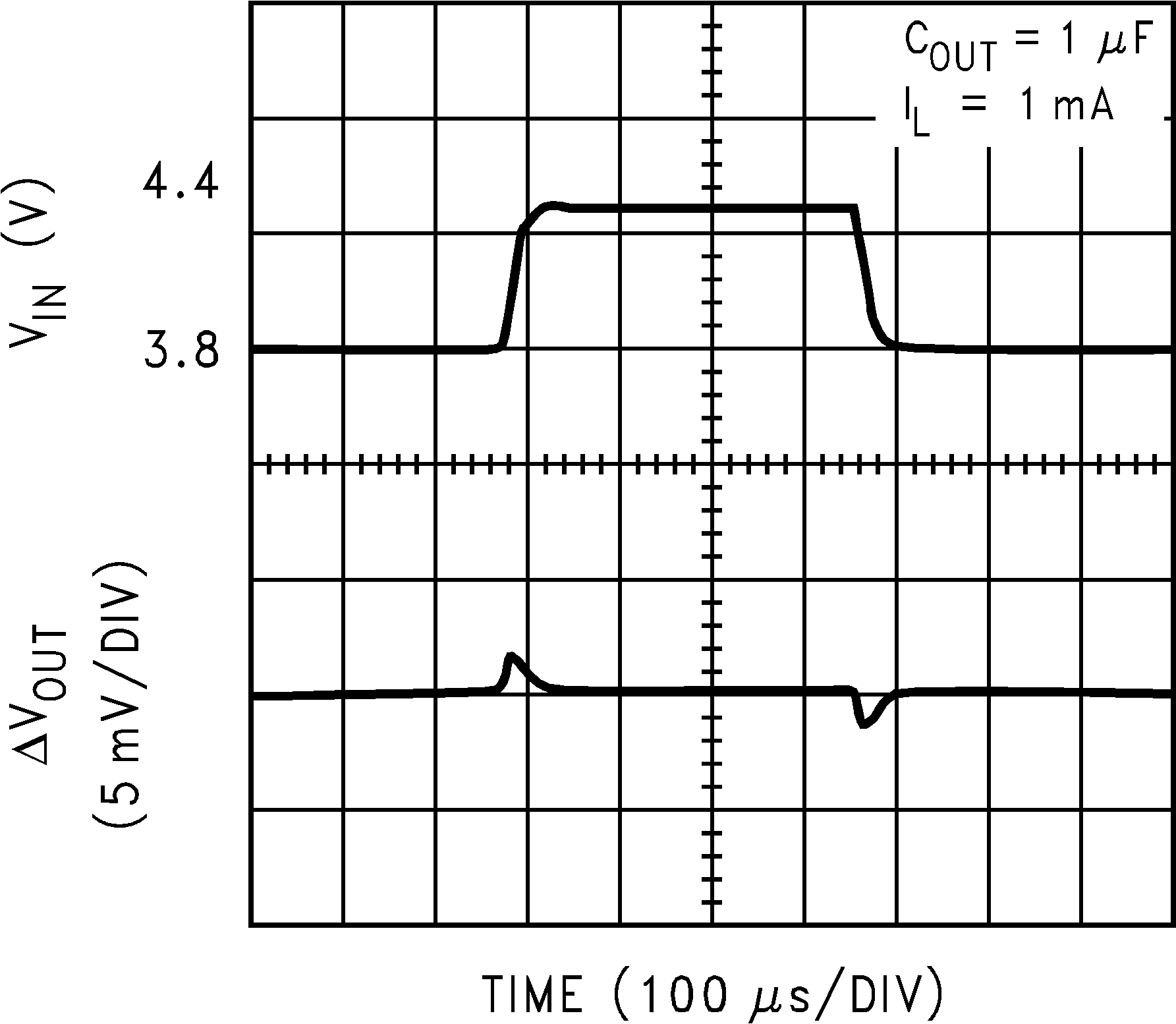
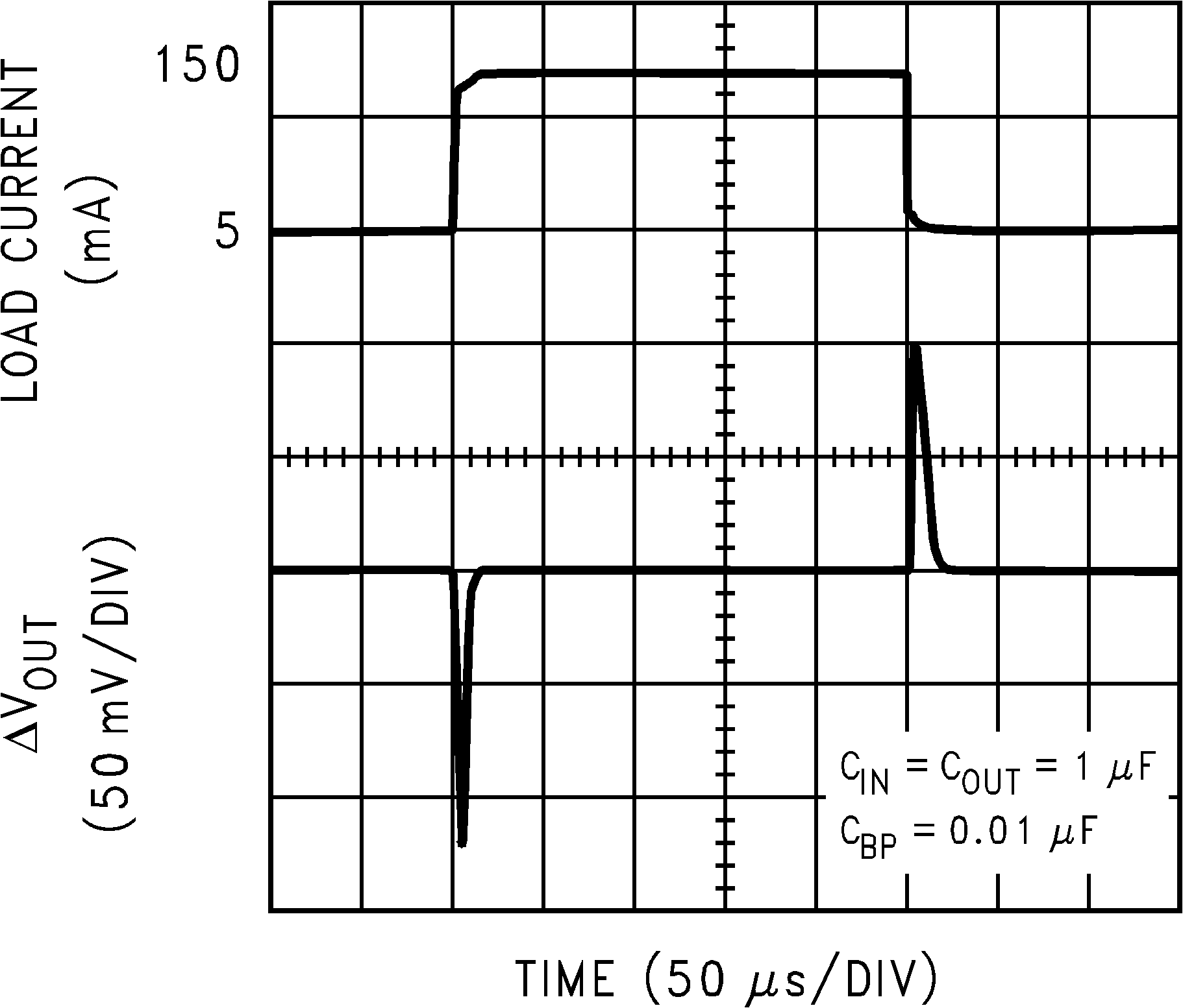
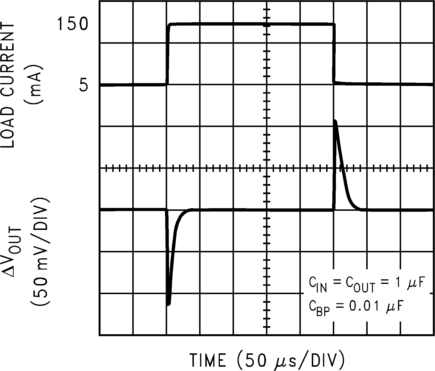
9.2.3 Application Curves

| VOUT = 2.8 V |

| VOUT = 1.8 V |

| VOUT = 2.8 V |