ZHCSAS0L January 2005 – December 2014 LP38691 , LP38691-Q1 , LP38693 , LP38693-Q1
PRODUCTION DATA.
- 1 特性
- 2 应用范围
- 3 说明
- 4 典型应用电路
- 5 修订历史记录
- 6 Pin Configuration and Functions
- 7 Specifications
- 8 Detailed Description
- 9 Application and Implementation
- 10Power Supply Recommendations
- 11Layout
- 12器件和文档支持
- 13机械封装和可订购信息
6 Pin Configuration and Functions
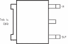
NDP Package
3-Pin TO-252
Top View
NDC Package
5-Pin SOT-223
Top View
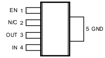
NC - No internal connection
NGG Package
6-Pin WSON With Exposed Thermal Pad
LP38691SD Top View
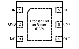
NC - No internal connection
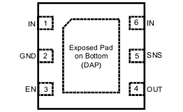
NGG Package
6-Pin WSON With Exposed Thermal Pad
LP38693SD Top View
Pin Functions
| PIN | I/O | DESCRIPTION | ||||
|---|---|---|---|---|---|---|
| NAME | TO-252 | WSON | SOT-223 | |||
| IN | 3 | 1, 6 | 1, 6 | 4 | I | This is the input supply voltage to the regulator. For WSON devices, both VIN pins must be tied together for full current operation (250mA maximum per pin). |
| GND | TAB | 2 | 2 | 5 | — | Circuit ground for the regulator. For the PFM and SOT-223 packages this is thermally connected to the die and functions as a heat sink when the soldered down to a large copper plane. |
| SNS | — | 5 | 5 | — | I | WSON Only - Output sense pin allows remote sensing at the load which will eliminate the error in output voltage due to voltage drops caused by the resistance in the traces between the regulator and the load. This pin must be tied to VOUT. |
| EN | — | — | 3 | 1 | I | The enable pin allows the part to be turned ON and OFF by pulling this pin high or low. |
| OUT | 1 | 4 | 4 | 3 | O | Regulated output voltage |
| DAP | — | √ | √ | — | — | WSON Only - The DAP (Exposed Pad) functions as a thermal connection when soldered to a copper plane. See WSON Mounting section for more information. |