ZHCSAS0L January 2005 – December 2014 LP38691 , LP38691-Q1 , LP38693 , LP38693-Q1
PRODUCTION DATA.
- 1 特性
- 2 应用范围
- 3 说明
- 4 典型应用电路
- 5 修订历史记录
- 6 Pin Configuration and Functions
- 7 Specifications
- 8 Detailed Description
- 9 Application and Implementation
- 10Power Supply Recommendations
- 11Layout
- 12器件和文档支持
- 13机械封装和可订购信息
11 Layout
11.1 Layout Guidelines
The dynamic performance of the LP3869x is dependent on the layout of the PCB. PCB layout practices that are adequate for typical LDOs may degrade the load regulation, PSRR, noise, or transient performance of the LP3869x.
Best performance is achieved by placing CIN and COUT on the same side of the PCB as the LP3869x, and as close as is practical to the package. The ground connections for CIN and COUT should be back to the LP3869x ground pin using as wide, and as short, a copper trace as is practical.
Connections using long trace lengths, narrow trace widths, and/or connections through vias should be avoided. These will add parasitic inductances and resistance that results in inferior performance especially during transient conditions.
A Ground Plane, either on the opposite side of a two-layer PCB, or embedded in a multi-layer PCB, is strongly recommended. This Ground Plane serves two purposes:
- Provides a circuit reference plane to assure accuracy.
- Provides a thermal plane to remove heat from the LP3869x WSON package through thermal vias under the package DAP.
11.1.1 WSON Mounting
The NGG0006A (No Pullback) 6-Lead WSON package requires specific mounting techniques which are detailed in the TI AN-1187 Application Report SNOA401. Referring to the section PCB Design Recommendations (Page 5), it should be noted that the pad style which should be used with the WSON package is the NSMD (non-solder mask defined) type. Additionally, it is recommended the PCB terminal pads to be 0.2-mm longer than the package pads to create a solder fillet to improve reliability and inspection.
The input current is split between two VIN pins, 1 and 6. The two VIN pins must be connected together to ensure that the device can meet all specifications at the rated current.
The thermal dissipation of the WSON package is directly related to the printed circuit board construction and the amount of additional copper area connected to the DAP.
The DAP (exposed pad) on the bottom of the WSON package is connected to the die substrate with a conductive die attach adhesive. The DAP has no direct electrical (wire) connection to any of the pins. There is a parasitic PN junction between the die substrate and the device ground. As such, it is strongly recommend that the DAP be connected directly to the ground at device lead 2 (that is, GND). Alternately, but not recommended, the DAP may be left floating (that is, no electrical connection). The DAP must not be connected to any potential other than ground.
11.2 Layout Example
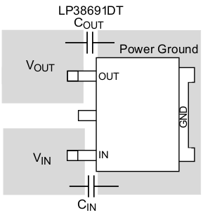 Figure 30. TO-252 Package
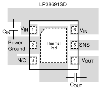 Figure 31. WSON LP38691D Package
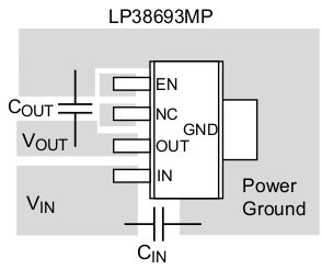
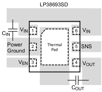 Figure 33. WSON LP38693SD Package