SNVS361E July 2007 – November 2015 LP38513
PRODUCTION DATA.
- 1 Features
- 2 Applications
- 3 Description
- 4 Revision History
- 5 Pin Configuration and Functions
- 6 Specifications
- 7 Detailed Description
- 8 Application and Implementation
- 9 Power Supply Recommendations
- 10Layout
- 11Device and Documentation Support
- 12Mechanical, Packaging, and Orderable Information
封装选项
机械数据 (封装 | 引脚)
散热焊盘机械数据 (封装 | 引脚)
- KTT|5
订购信息
6 Specifications
6.1 Absolute Maximum Ratings
over operating free-air temperature range (unless otherwise noted)(1)(2)| MIN | MAX | UNIT | ||
|---|---|---|---|---|
| IN pin voltage (survival) | −0.3 | 6 | V | |
| EN pin voltage (survival) | −0.3 | 6 | V | |
| OUT pin Voltage (survival) | −0.3 | 6 | V | |
| ERROR pin voltage (survival) | −0.3 | 6 | V | |
| IOUT (Survival) | Internally limited | |||
| Power dissipation(3) | Internally limited | |||
| Storage temperature, Tstg | −65 | 150 | °C | |
(1) Stresses beyond those listed under Absolute Maximum Ratings may cause permanent damage to the device. These are stress ratings only, which do not imply functional operation of the device at these or any other conditions beyond those indicated under Recommended Operating Conditions. Exposure to absolute-maximum-rated conditions for extended periods may affect device reliability.
(2) If Military/Aerospace specified devices are required, contact the TI Sales Office/ Distributors for availability and specifications.
6.2 ESD Ratings
| VALUE | UNIT | |||
|---|---|---|---|---|
| V(ESD) | Electrostatic discharge | Human-body model (HBM), per ANSI/ESDA/JEDEC JS-001(1) | ±2000 | V |
(1) JEDEC document JEP155 states that 500-V HBM allows safe manufacturing with a standard ESD control process.
6.3 Recommended Operating Conditions
over operating free-air temperature range (unless otherwise noted)(1)| MIN | NOM | MAX | UNIT | ||
|---|---|---|---|---|---|
| Input supply voltage, VIN | 2.25 | 5.5 | V | ||
| Enable input voltage, VEN | 0 | 5.5 | V | ||
| ERROR pin voltage | 0 | VIN | V | ||
| Output current (DC) | 0 | 3 | mA/A | ||
| Junction temperature(2) | −40 | 125 | °C | ||
(1) Stresses beyond those listed under Absolute Maximum Ratings may cause permanent damage to the device. These are stress ratings only, which do not imply functional operation of the device at these or any other conditions beyond those indicated under Recommended Operating Conditions. Exposure to absolute-maximum-rated conditions for extended periods may affect device reliability.
(2) Device operation must be evaluated, and derated as needed, based on ambient temperature (TA), power dissipation (PD), maximum allowable operating junction temperature (TJ(MAX)), and package thermal resistance (RθJA).
6.4 Thermal Information
| THERMAL METRIC(1) | LP38513 | UNIT | ||
|---|---|---|---|---|
| NDH (TO-220) | KTT (DDPAK/TO-263) | |||
| 5 PINS | 5 PINS | |||
| RθJA | Junction-to-ambient thermal resistance | 31.9 | 32.9 | °C/W |
| RθJC(top) | Junction-to-case (top) thermal resistance | 43.7 | 37.6 | °C/W |
| RθJB | Junction-to-board thermal resistance | 16.4 | 18.9 | °C/W |
| ψJT | Junction-to-top characterization parameter | 8.3 | 5.7 | °C/W |
| ψJB | Junction-to-board characterization parameter | 16.4 | 17.3 | °C/W |
| RθJC(bot) | Junction-to-case (bottom) thermal resistance | 1.2 | 1.0 | °C/W |
(1) For more information about traditional and new thermal metrics, see the Semiconductor and IC Package Thermal Metrics application report, SPRA953.
6.5 Electrical Characteristics
Unless otherwise specified: VIN = 2.5 V, IOUT = 10 mA, CIN = 10 µF, COUT = 10 µF, VEN = 2 V, and limits apply for TJ = 25°C. Minimum and Maximum limits are specified through test, design, or statistical correlation. Typical values represent the most likely parametric norm at TJ = 25°C, and are provided for reference purposes only.| PARAMETER | TEST CONDITIONS | MIN | TYP | MAX | UNIT | |
|---|---|---|---|---|---|---|
| VOUT | Output voltage tolerance(1) | 2.25 V ≤ VIN ≤ 5.5 V 10 mA ≤ IOUT ≤ 3 A |
–1.6% | 0% | 1.6% |
|
| 2.25 V ≤ VIN ≤ 5.5 V 10 mA ≤ IOUT ≤ 3 A TJ = –40°C to +125°C |
–4.1% | 2.6% | ||||
| 2.25V ≤ VIN ≤ 5.5V 10 mA ≤ IOUT ≤ 3A 0°C ≤ TJ ≤ 125°C |
–2.6% | 0% | 2.6% | |||
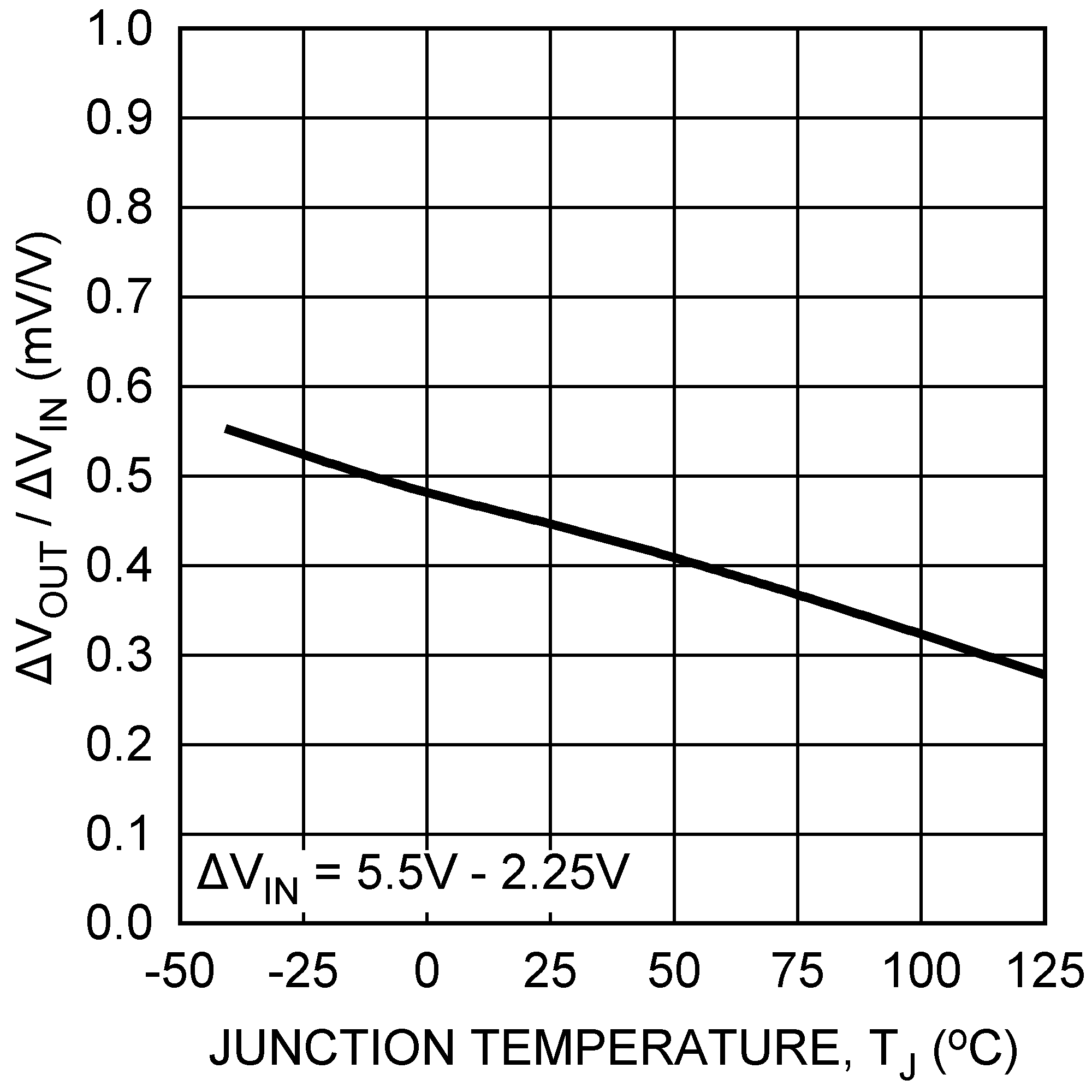
| ΔVOUT/ΔVIN | Output voltage line regulation(1)(2) | 2.25 V ≤ VIN ≤ 5.5 V | 0.03 | %/V | ||
| 2.25 V ≤ VIN ≤ 5.5 V TJ = –40°C to +125°C |
0.06 | |||||
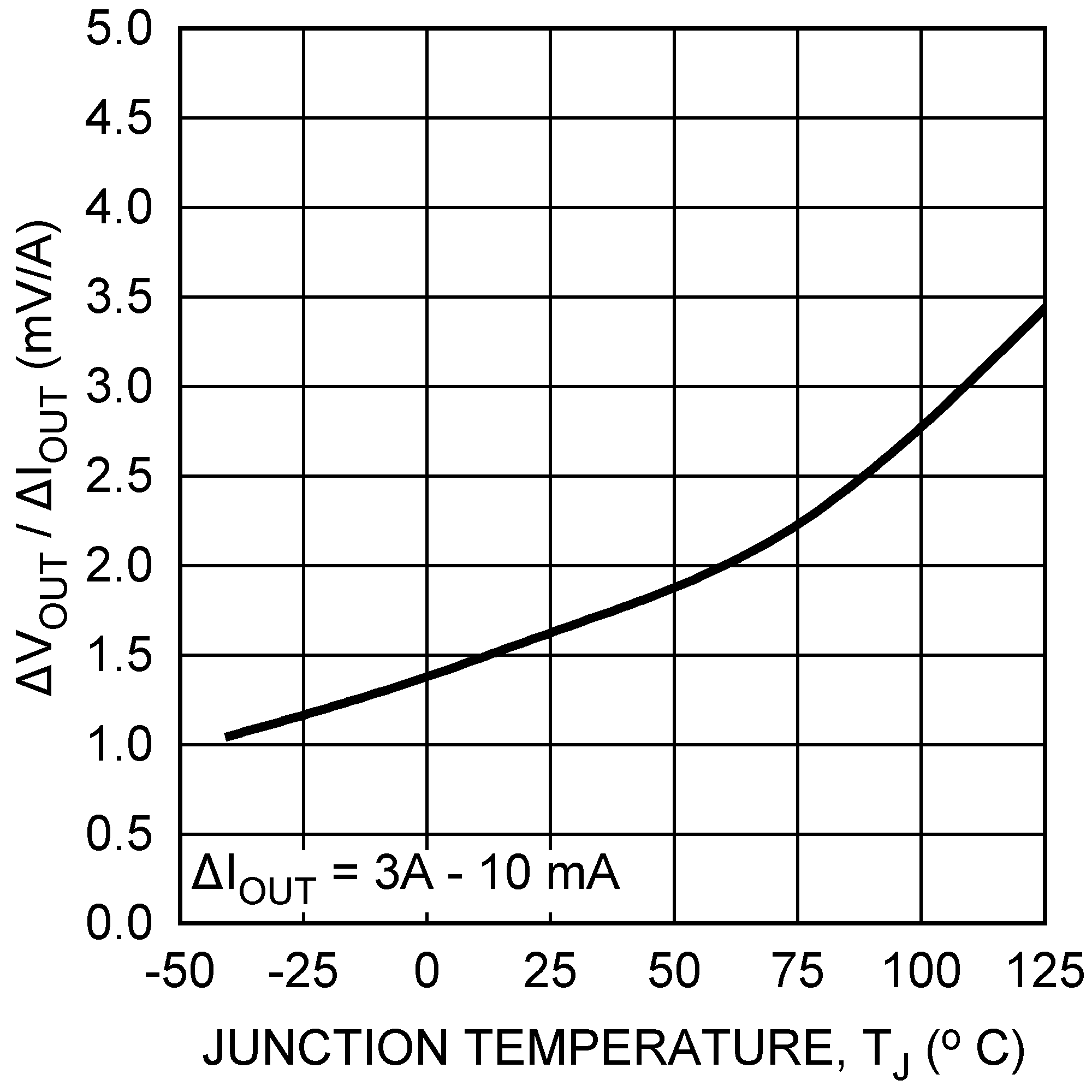
| ΔVOUT/ΔIOUT | Output voltage load regulation(1)(3) | 10 mA ≤ IOUT ≤ 3 A | 0.1 | %/A | ||
| 10 mA ≤ IOUT ≤ 3 A TJ = –40°C to +125°C |
0.2 | |||||
| VDO | Dropout voltage(4) | IOUT = 3 A, TJ = –40°C to +125°C | 425 | mV | ||
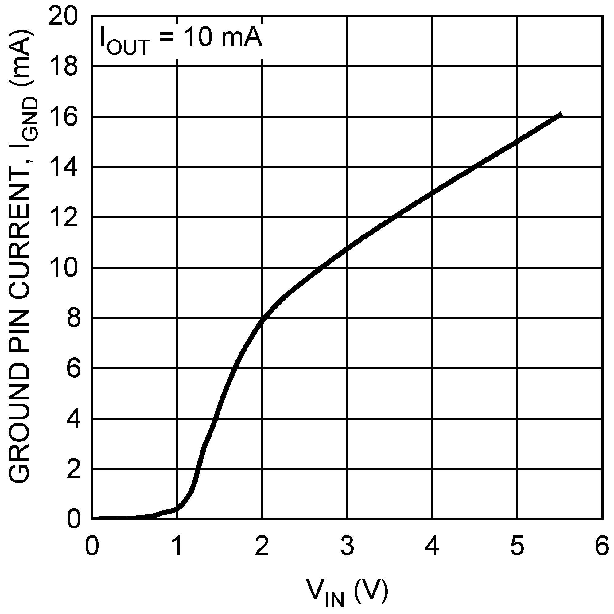
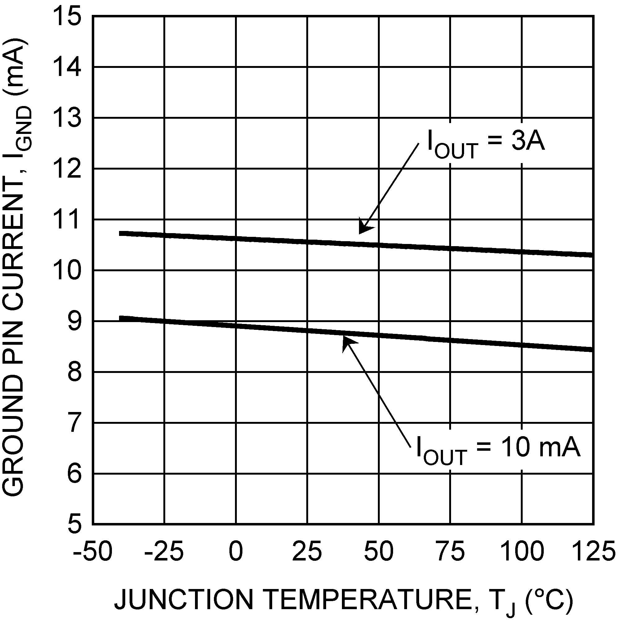
| IGND | Ground pin current, output enabled | IOUT = 10 mA, ERROR pin = GND | 10 | 12 | mA | |
| IOUT = 10 mA, ERROR pin = GND TJ = –40°C to +125°C |
15 | |||||
| IOUT = 3 A, ERROR pin = GND | 12 | 15 | ||||
| IOUT = 3 A, ERROR pin = GND TJ = –40°C to +125°C |
20 | |||||
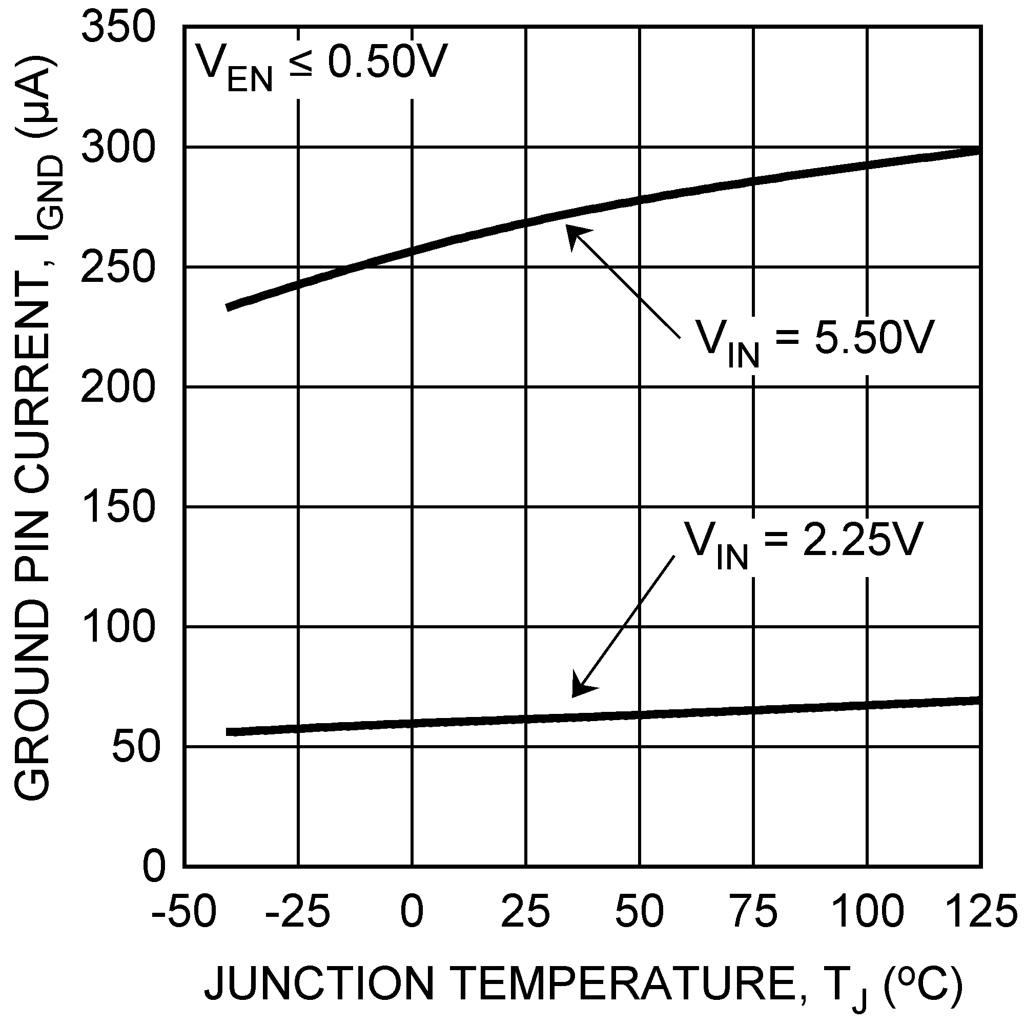
| Ground pin current, output disabled | VEN = 0.5 V, ERROR pin = GND | 60 | 100 | µA | ||
| VEN = 0.5 V, ERROR pin = GND TJ = –40°C to +125°C |
110 | |||||
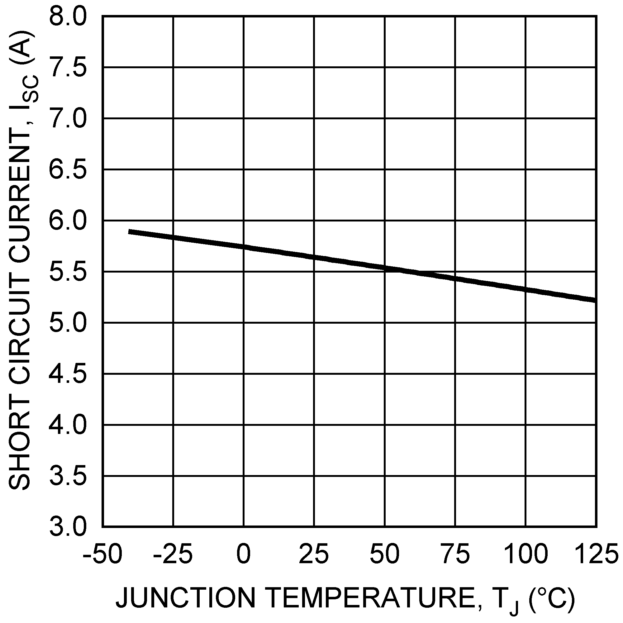
| ISC | Short-circuit current | VOUT = 0 V | 5.6 | A | ||
| ENABLE INPUT | ||||||
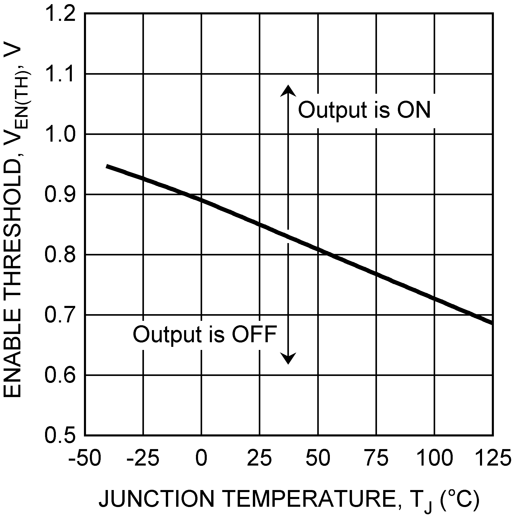
| VEN(TH) | Enable on/off threshold | VEN rising from 0 V until the output turns to an ON state, or VEN falling from ≥ 2 V until the output turns to an OFF state | 0.74 | 0.85 | 0.92 | V |
| VEN rising from 0 V until the output turns to an ON state, or VEN falling from ≥ 2 V until the output turns to an OFF state TJ = –40°C to +125°C |
0.56 | 1 | ||||
| td(OFF) | Turnoff delay | Time from VEN < VEN(TH) to VOUT = OFF, ILOAD = 3 A | 5 | µs | ||
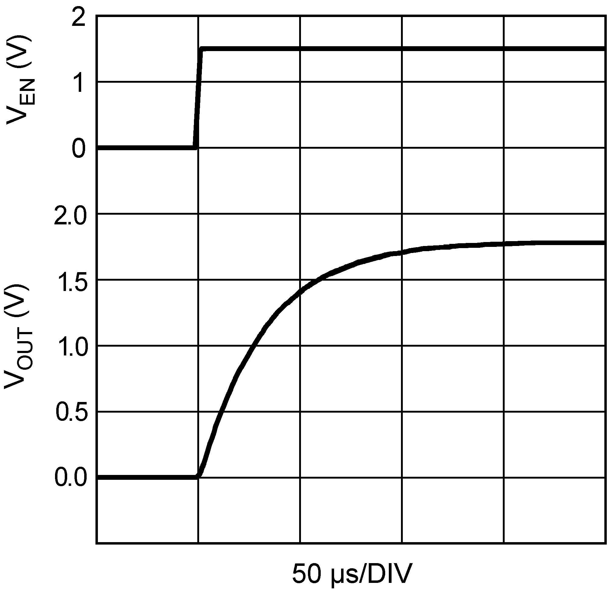
| td(ON) | Turnon delay | Time from VEN >VEN(TH) to VOUT = ON, ILOAD = 3 A | 5 | |||
| IEN | EN pin current | VEN = VIN | 1 | nA | ||
| VEN = 0 V | –1 | |||||
| ERROR FLAG | ||||||
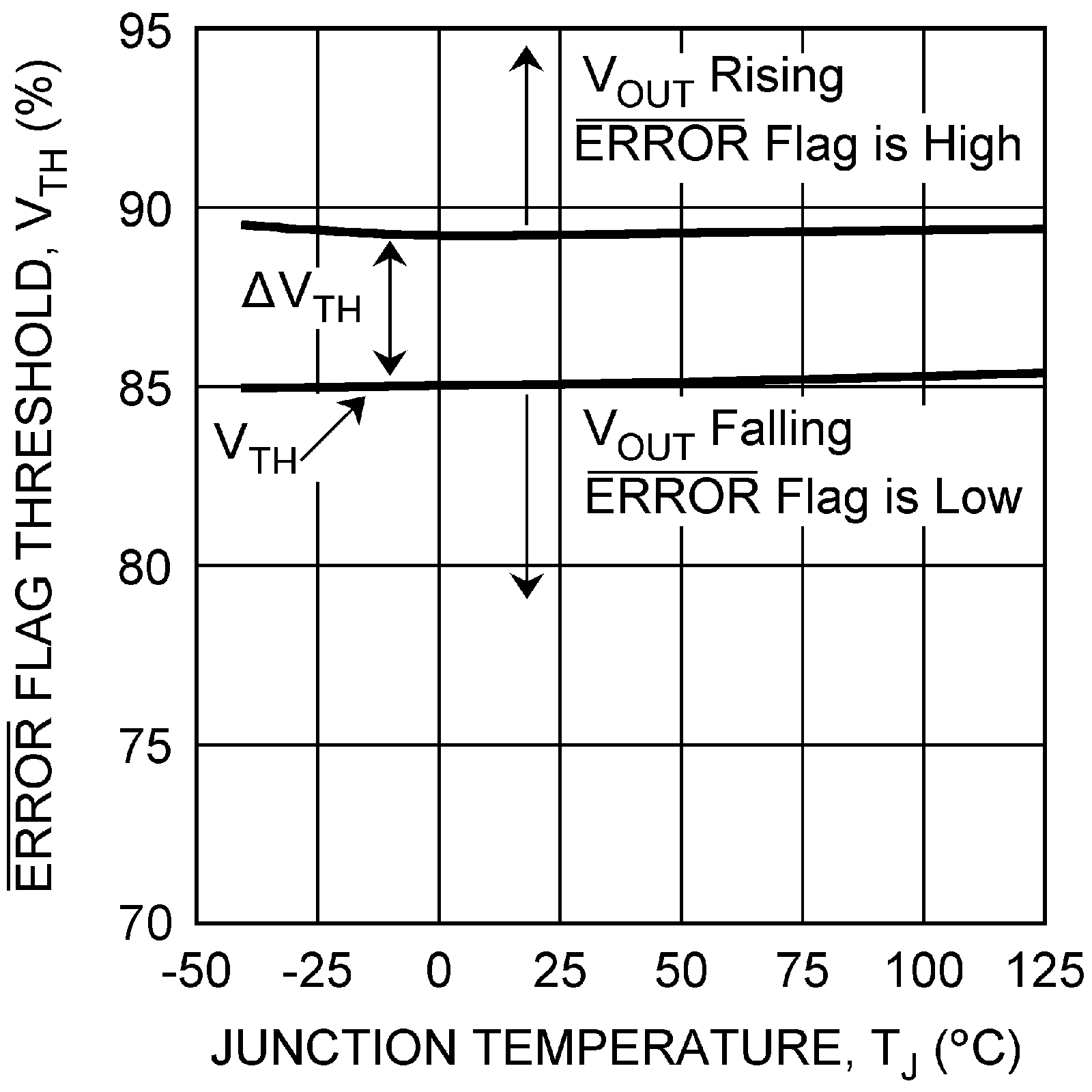
| VTH | ERROR flag threshold(5) | VOUT falling from VOUT(NOM) until ERROR flag goes low | 85% | |||
| VOUT falling from VOUT(NOM) until ERROR flag goes low TJ = –40°C to +125°C |
77% | 94% | ||||
| ΔVTH | ERROR flag threshold hysteresis(5) | VOUT rising from VTH until ERROR flag goes high | 4% | |||
| VOUT rising from VTH until ERROR flag goes high TJ = –40°C to +125°C |
2.2% | 5.8% | ||||
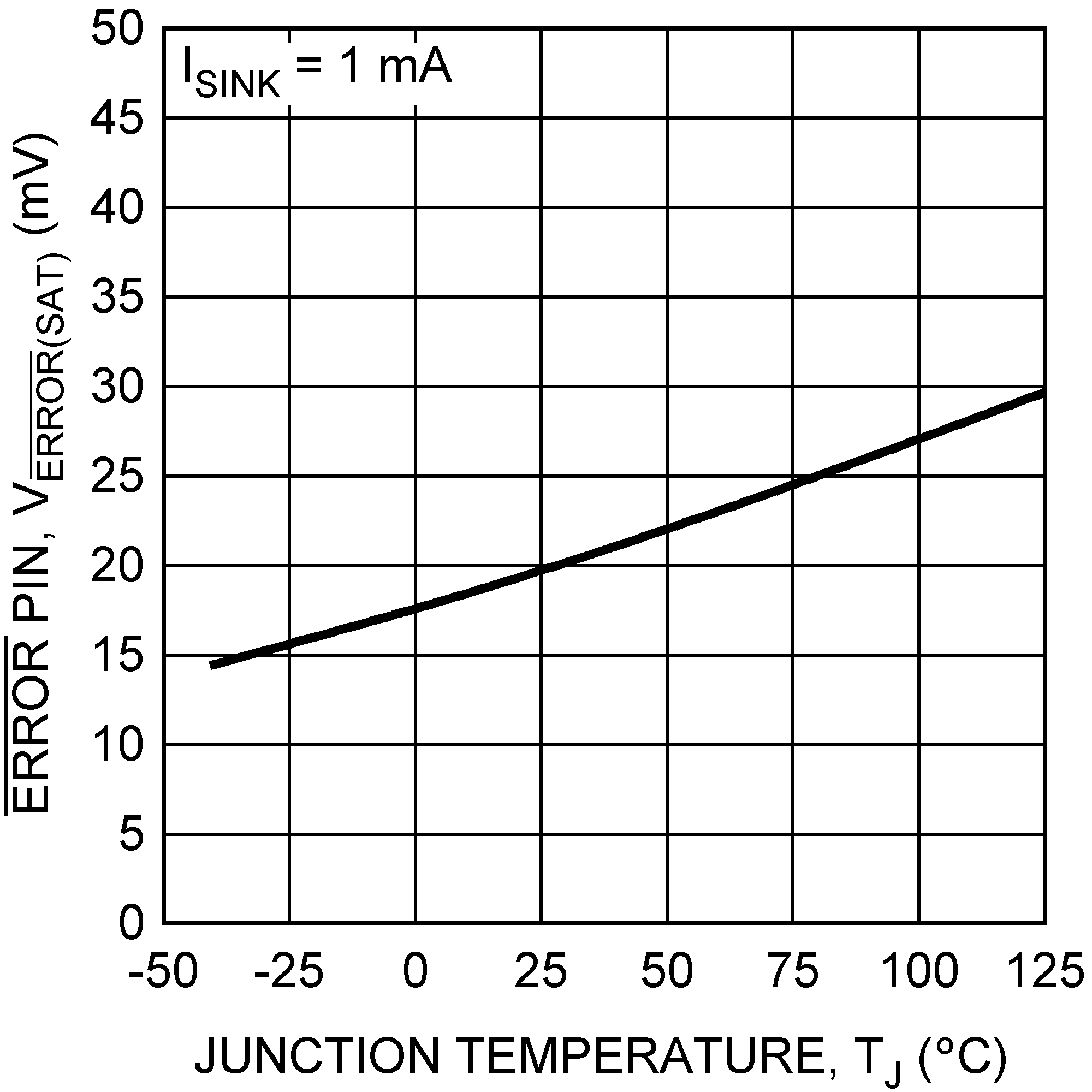
| VERROR(SAT) | ERROR flag saturation voltage | ISINK = 1 mA | 20 | mV | ||
| ISINK = 1 mA, TJ = –40°C to +125°C | 100 | |||||
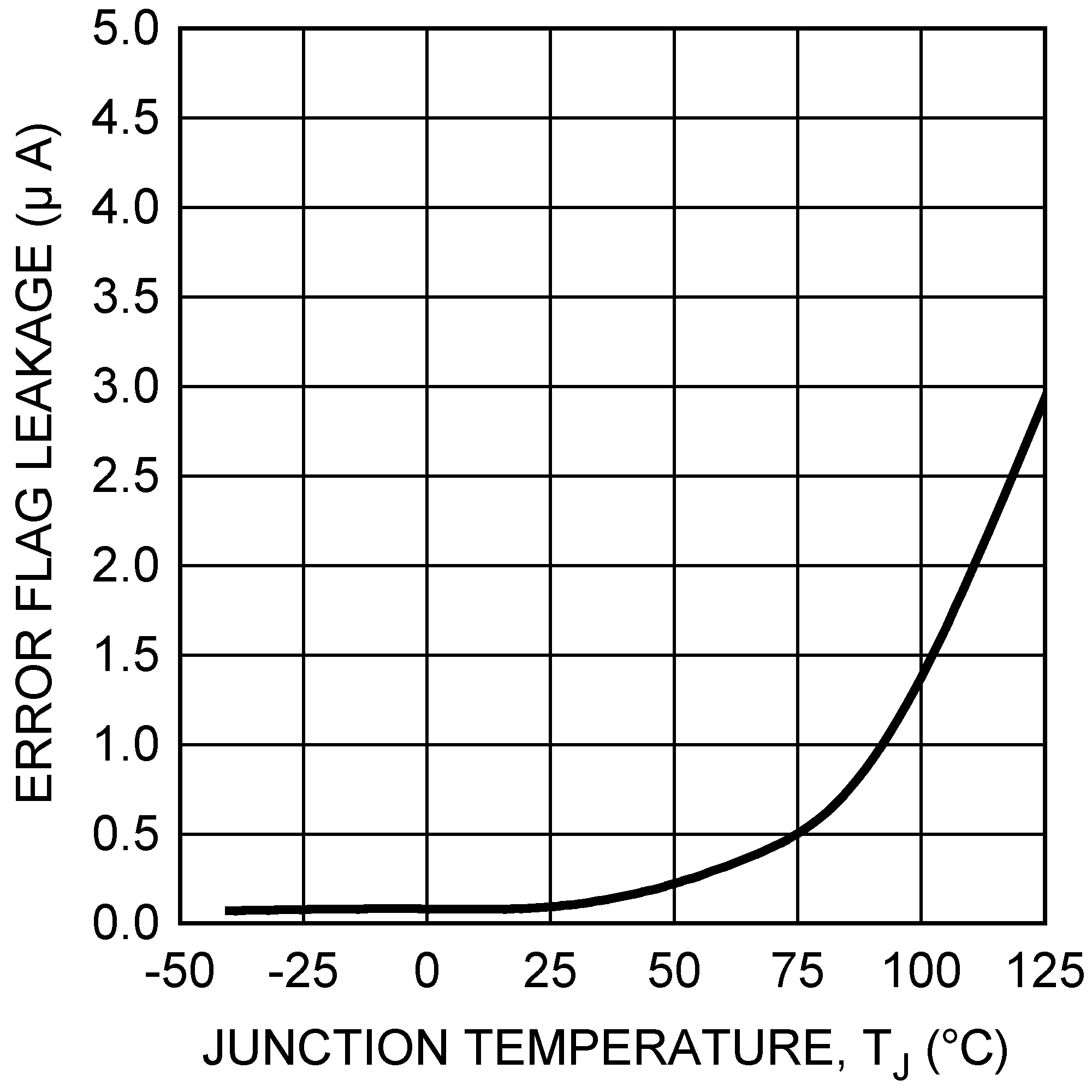
| Ilk | ERROR flag pin leakage current | VERROR = 5.5 V | 100 | nA | ||
| td | ERROR flag delay time | 1 | µs | |||
| AC PARAMETERS | ||||||
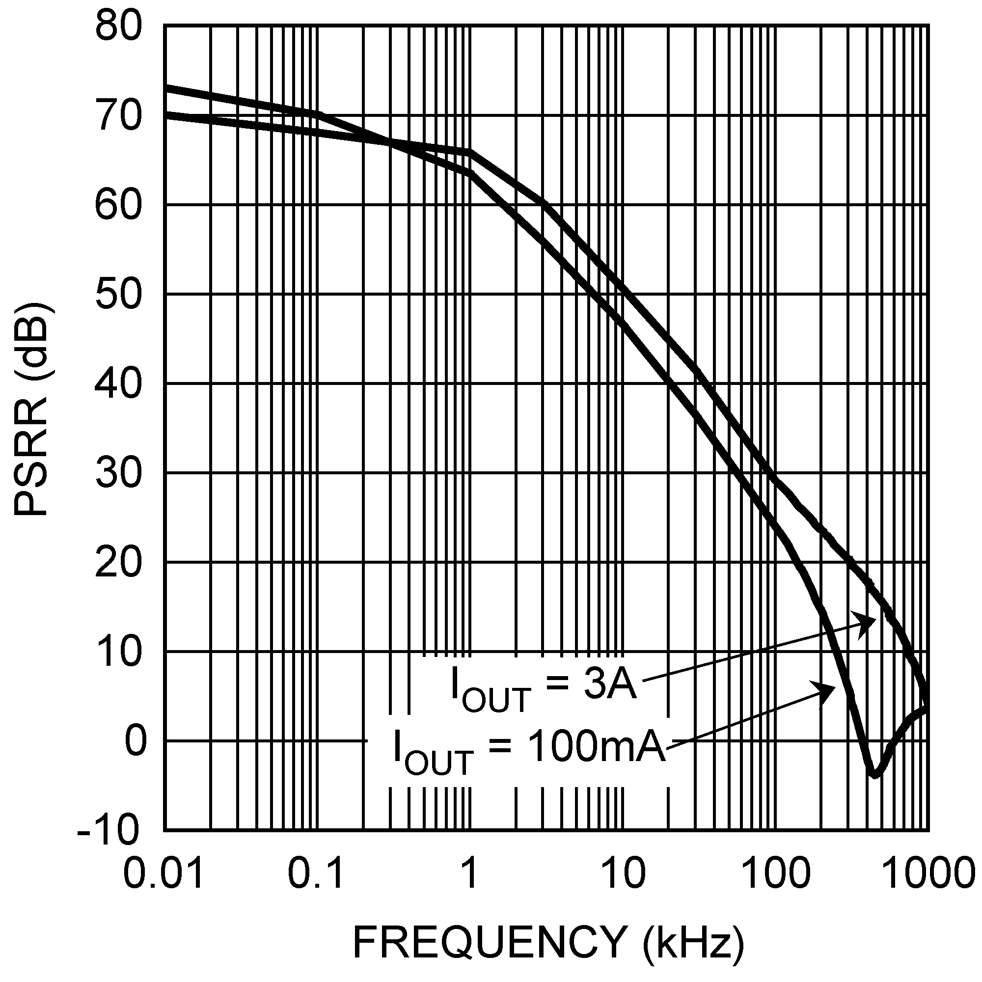
| PSRR | Ripple rejection | VIN = 2.5 V, ƒ = 120 Hz | 73 | dB | ||
| VIN = 2.5 V, ƒ = 1 kHz | 70 | |||||
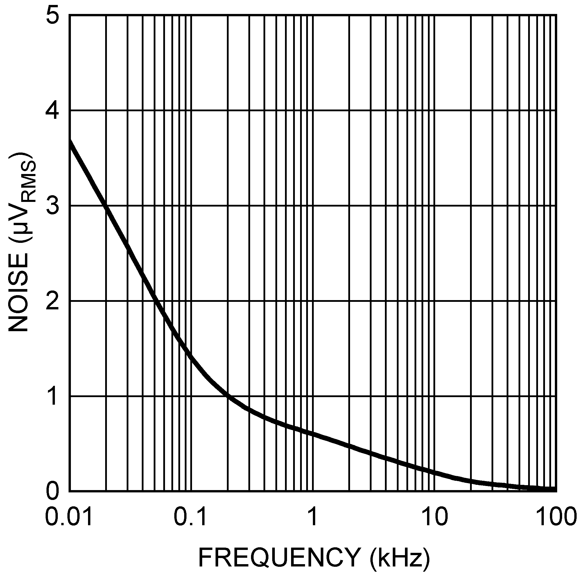
| ρn(l/f) | Output noise density | ƒ = 120 Hz | 0.8 | µV/√Hz | ||
| en | Output noise voltage | BW = 100 Hz – 100 kHz, VOUT = 1.8 V | 45 | µVRMS | ||
| THERMAL CHARACTERISTICS | ||||||
| TSD | Thermal shutdown | TJ rising | 165 | °C | ||
| ΔTSD | Thermal shutdown hysteresis | TJ falling from TSD | 10 | |||
(1) The line and load regulation specification contains only the typical number. However, the limits for line and load regulation are included in the output voltage tolerance specification.
(2) Output voltage line regulation is defined as the change in output voltage from the nominal value due to change in the voltage at the input.
(3) Output voltage load regulation is defined as the change in output voltage from the nominal value due to change in the load current at the output.
(4) Dropout voltage (VDO) is typically defined as the input to output voltage differential (VIN – VOUT) where the input voltage is low enough to cause the output voltage to drop 2% from the nominal value. For the LP38513, the minimum operating voltage of 2.25 V is the limiting factor, and the maximum dropout voltage is defined as: VDO(MAX) = VIN(MIN) – VOUT(MIN) = (2.25 V – (1.8 V × 95.9%) = 524 mV).
(5) The ERROR flag thresholds are specified as percentage of the nominal regulated output voltage. See Application and Implementation section.
6.6 Typical Characteristics
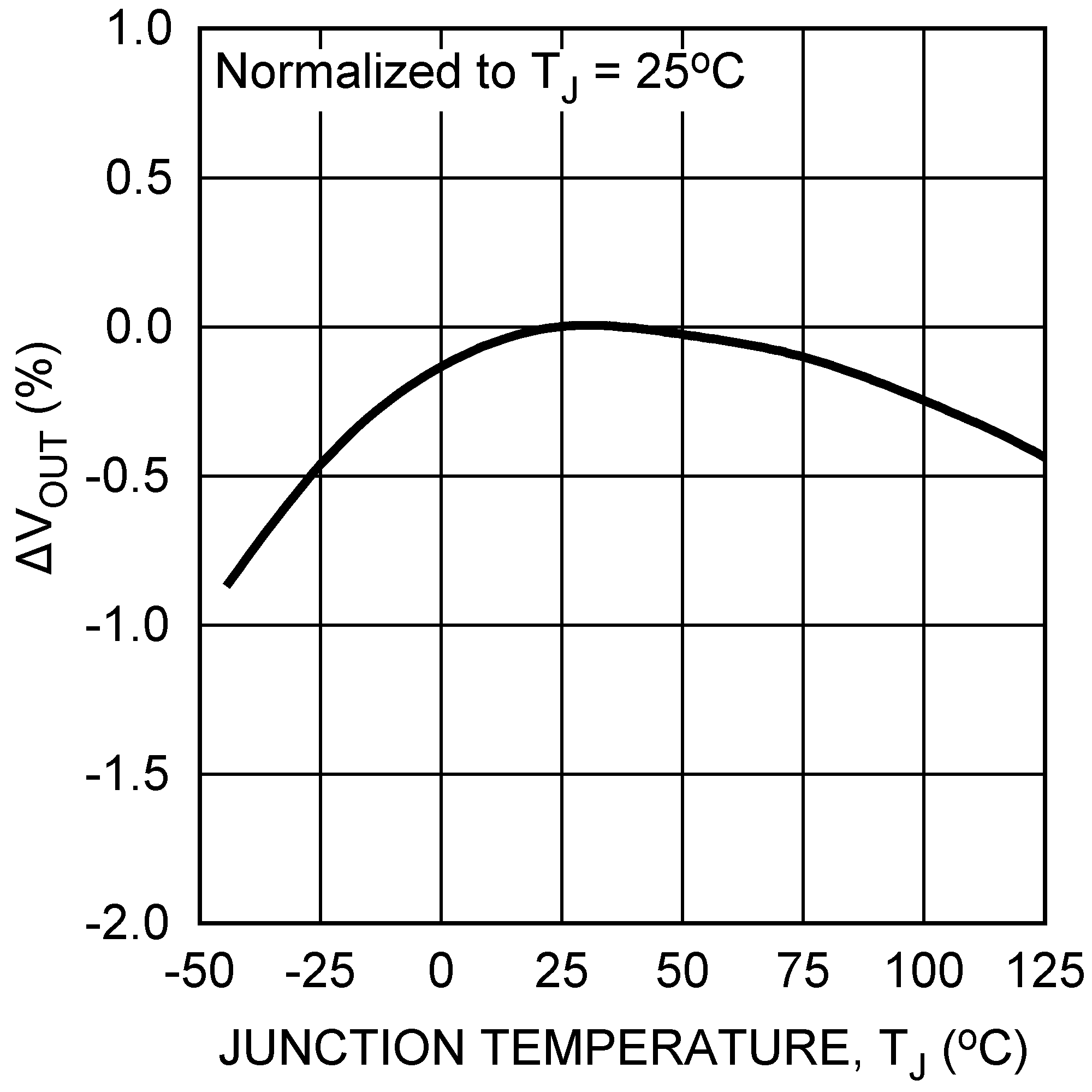
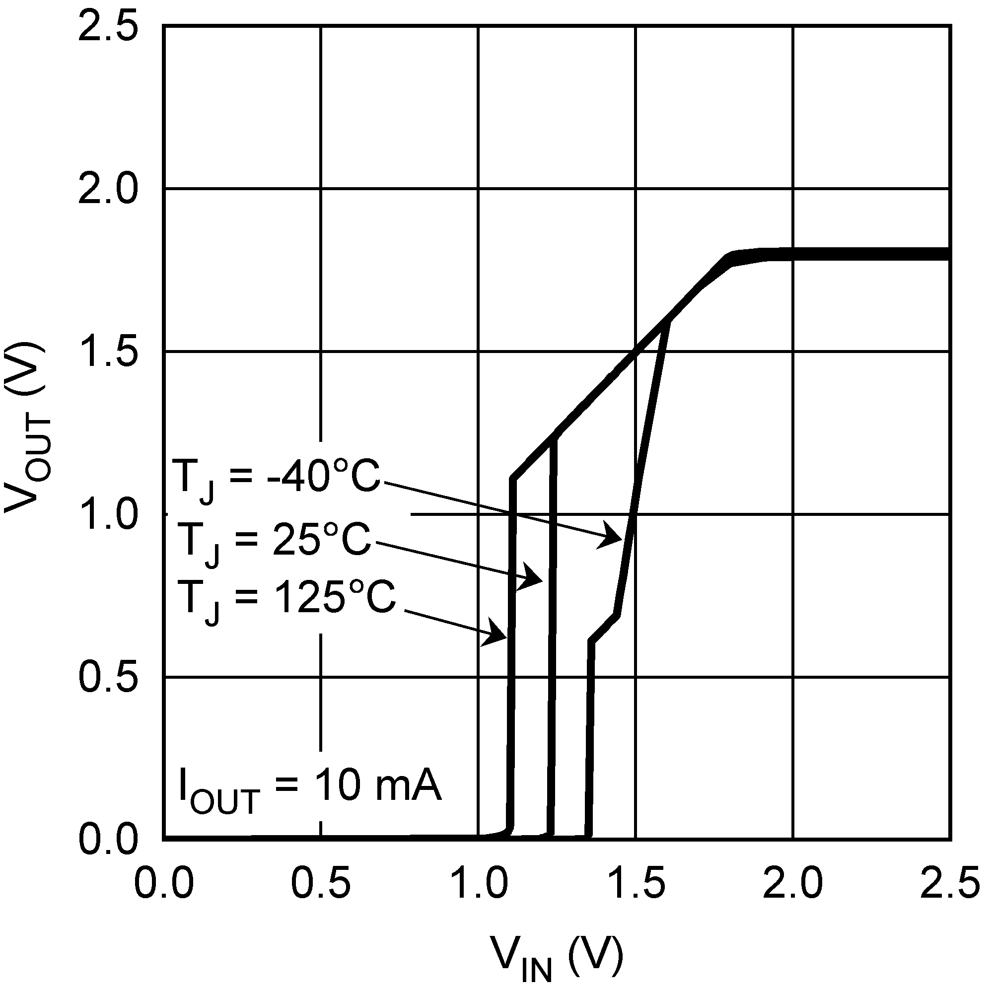
Unless otherwise specified: TJ = 25°C, VIN = 2.5V, VEN = 2 V, CIN = 10 µF, COUT = 10 µF, IOUT = 10 mA.