SNVS361E July 2007 – November 2015 LP38513
PRODUCTION DATA.
- 1 Features
- 2 Applications
- 3 Description
- 4 Revision History
- 5 Pin Configuration and Functions
- 6 Specifications
- 7 Detailed Description
- 8 Application and Implementation
- 9 Power Supply Recommendations
- 10Layout
- 11Device and Documentation Support
- 12Mechanical, Packaging, and Orderable Information
封装选项
机械数据 (封装 | 引脚)
散热焊盘机械数据 (封装 | 引脚)
- KTT|5
订购信息
8 Application and Implementation
NOTE
Information in the following applications sections is not part of the TI component specification, and TI does not warrant its accuracy or completeness. TI’s customers are responsible for determining suitability of components for their purposes. Customers should validate and test their design implementation to confirm system functionality.
8.1 Application Information
The typical application of the LP38513 includes microprocessor supplies, bus terminators, post regulators, and battery-powered application. Figure 18 shows the typical application circuit for LP38513. The input and output capacitances may need to be increased above the 10-µF minimum for some applications.
8.2 Typical Application
 Figure 18. LP38513 Typical Application
8.2.1 Design Requirements
For the typical LP38513 ultra-low-dropout linear regulator applications, use the parameters listed in Table 1.
Table 1. Design Parameters
| DESIGN PARAMETER | EXAMPLE VALUE |
|---|---|
| Minimum input voltage | 2.25 V |
| Output voltage | 1.8 V |
| Output current | 0 mA to 3 A |
8.2.2 Detailed Design Procedure
8.2.2.1 External Capacitors
Like any low-dropout regulator, external capacitors are required to assure stability. These capacitors must be correctly selected for proper performance.
8.2.2.1.1 Input Capacitor
A ceramic input capacitor of at least 10 µF is required. For general usage across all load currents and operating conditions, a 10-µF ceramic input capacitor provides satisfactory performance.
8.2.2.1.2 Output Capacitor
A ceramic capacitor with a minimum value of 10 µF is required at the output pin for loop stability. It must be located less than 1 cm from the device and connected directly to the OUT and GND pin using traces which have no other currents flowing through them. As long as the minimum of 10 µF ceramic is met, there is no limitation on any additional capacitance.
X7R and X5R dielectric ceramic capacitors are strongly recommended, as they typically maintain a capacitance range within ±20% of nominal over full operating ratings of temperature and voltage; they are typically larger and more costly than Z5U/Y5U types for a given voltage and capacitance.
Z5U and Y5V dielectric ceramics are not recommended as the capacitance will drop severely with applied voltage. A typical Z5U or Y5V capacitor can lose 60% of its rated capacitance with half of the rated voltage applied to it. The Z5U and Y5V also exhibit a severe temperature effect, losing more than 50% of nominal capacitance at high and low limits of the temperature range.
8.2.2.2 Reverse Voltage
A reverse voltage condition will exist when the voltage at the OUT pin is higher than the voltage at the IN pin. Typically this happens when VIN is abruptly taken low and COUT continues to hold a sufficient charge such that the input to output voltage becomes reversed. A less common condition is when an alternate voltage source is connected to the output.
There are two possible paths for current to flow from the OUT pin back to the input during a reverse voltage condition.
While VIN is high enough to keep the control circuity alive, and the EN pin is above the VEN(ON) threshold, the control circuitry attempts to regulate the output voltage. Because the input voltage is less than the output voltage the control circuit drives the gate of the pass element to the full ON condition when the output voltage begins to fall. In this condition, reverse current will flow from the OUT pin to the IN pin, limited only by the RDS(ON) of the pass element and the output-to-input voltage differential. Discharging an output capacitor up to 1000 µF in this manner does not damage the device as the current rapidly decays. However, continuous reverse current must be avoided.
The internal PFET pass element in the LP38513 has an inherent parasitic diode. During normal operation, the input voltage is higher than the output voltage, and the parasitic diode is reverse biased. However, if the output-voltage-to-input-voltage differential is more than 500 mV (typical), the parasitic diode becomes forward biased, and current flows from the OUT pin to the input through the diode. The current in the parasitic diode must be limited to less than 1-A continuous and 5-A peak.
If used in a dual-supply system where the regulator output load is returned to a negative supply, the OUT pin must be diode clamped to ground. A Schottky diode is recommended for this protective clamp.
8.2.2.3 Power Dissipation
A heat sink may be required depending on the maximum power dissipation (PD(MAX)), maximum ambient temperature (TA(MAX))of the application, and the thermal resistance (RθJA) of the package. Under all possible conditions, the junction temperature (TJ) must be within the range specified in the Recommended Operating Conditions. The total power dissipation of the device is given by:
where
- IGND is the operating ground current of the device (specified under Electrical Characteristics).
The maximum allowable junction temperature rise (ΔTJ) depends on the maximum expected ambient temperature (TA(MAX)) of the application, and the maximum allowable junction temperature (TJ(MAX)):
The maximum allowable value for junction-to-ambient thermal resistance, RθJA, can be calculated using the formula:
Knowing the device power dissipation and proper sizing of the thermal plane connected to the tab or pad is critical to ensuring reliable operation. Device power dissipation depends on input voltage, output voltage, and load conditions and can be calculated with Equation 4.
Power dissipation can be minimized, and greater efficiency can be achieved, by using the lowest available voltage drop option that would still be greater than the dropout voltage (VDO). However, keep in mind that higher voltage drops result in better dynamic (that is, PSRR and transient) performance.
The maximum allowable junction temperature (TJ(MAX)) determines maximum power dissipation allowed (PD(MAX)) for the device package.
Power dissipation and junction temperature are most often related by the junction-to-ambient thermal resistance (RθJA) of the combined PCB and device package and the temperature of the ambient air (TA), according to Equation 5 or Equation 6:
Unfortunately, this RθJA is highly dependent on the heat-spreading capability of the particular PCB design, and therefore varies according to the total copper area, copper weight, and location of the planes. The RθJA recorded in Thermal Information is determined by the specific EIA/JEDEC JESD51-7 standard for PCB and copper-spreading area, and is to be used only as a relative measure of package thermal performance. For a well-designed thermal layout, RθJA is actually the sum of the package junction-to-case (bottom) thermal resistance (RθJCbot) plus the thermal resistance contribution by the PCB copper area acting as a heat sink.
8.2.2.4 Estimating Junction Temperature
The EIA/JEDEC standard recommends the use of psi (Ψ) thermal characteristics to estimate the junction temperatures of surface mount devices on a typical PCB board application. These characteristics are not true thermal resistance values, but rather package specific thermal characteristics that offer practical and relative means of estimating junction temperatures. These psi metrics are determined to be significantly independent of copper-spreading area. The key thermal characteristics (ΨJT and ΨJB) are given in Thermal Information and are used in accordance with Equation 7 or Equation 8.
where
- PD(MAX) is explained in Equation 4.
- TTOP is the temperature measured at the center-top of the device package.
where
- PD(MAX) is explained in Equation 4.
- TBOARD is the PCB surface temperature measured 1-mm from the device package and centered on the package edge.
For more information about the thermal characteristics ΨJT and ΨJB, see the TI Application Report: Semiconductor and IC Package Thermal Metrics (SPRA953), available for download at www.ti.com.
For more information about measuring TTOP and TBOARD, see the TI Application Report: Using New Thermal Metrics (SBVA025), available for download at www.ti.com.
For more information about the EIA/JEDEC JESD51 PCB used for validating RθJA, see the TI Application Report: Thermal Characteristics of Linear and Logic Packages Using JEDEC PCB Designs (SZZA017), available for download at www.ti.com.
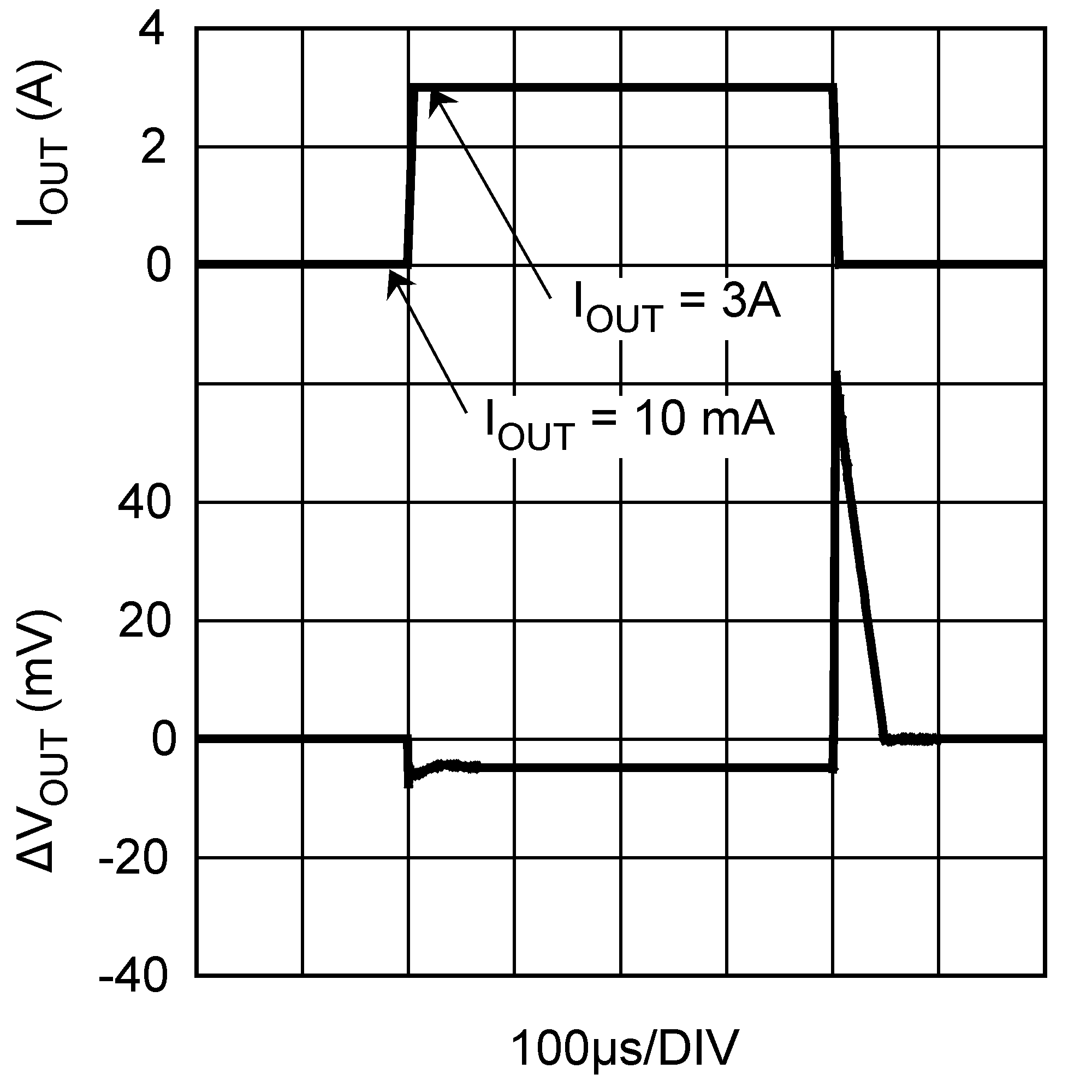
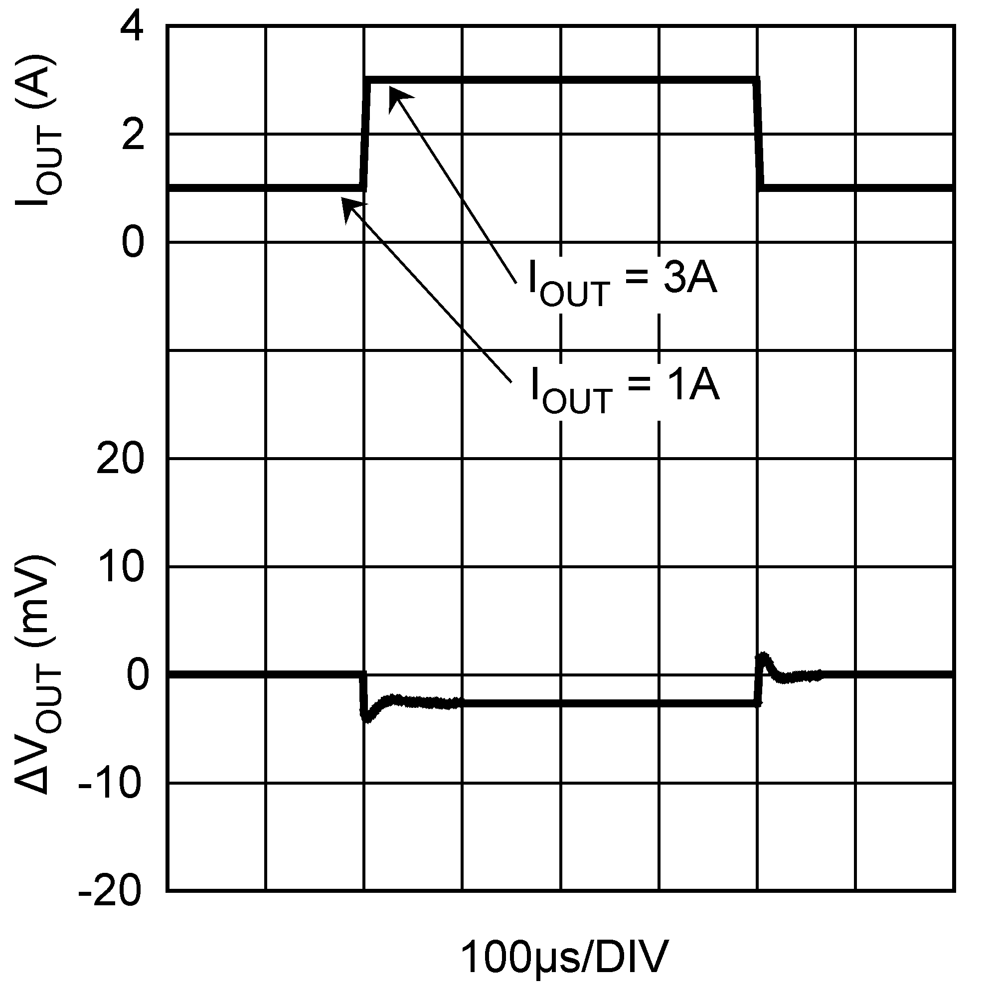
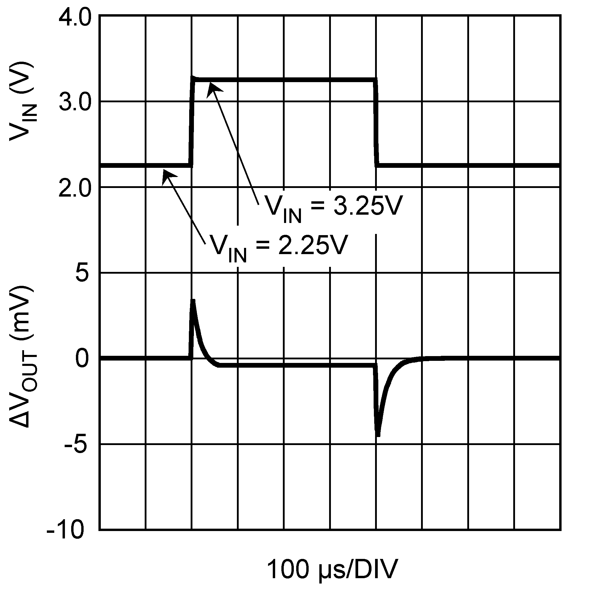
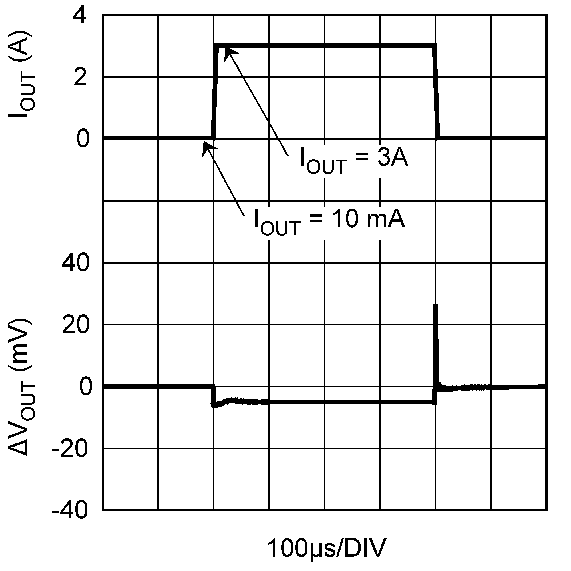
8.2.3 Application Curves

| 10 mA to 3 A | COUT = 10 µF Ceramic | |

| 10 mA to 3 A | COUT = 10 µF Ceramic | |


| 10 mA to 3 A | COUT = 10 µF ceramic + 100 µF aluminum | |

| 10 mA to 3 A | COUT = 10 µF Ceramic + 100 µF Aluminum | |