SNVS361E July 2007 – November 2015 LP38513
PRODUCTION DATA.
- 1 Features
- 2 Applications
- 3 Description
- 4 Revision History
- 5 Pin Configuration and Functions
- 6 Specifications
- 7 Detailed Description
- 8 Application and Implementation
- 9 Power Supply Recommendations
- 10Layout
- 11Device and Documentation Support
- 12Mechanical, Packaging, and Orderable Information
封装选项
机械数据 (封装 | 引脚)
散热焊盘机械数据 (封装 | 引脚)
- KTT|5
订购信息
7 Detailed Description
7.1 Overview
The LP38513 is a fast response, ultra-low-dropout linear regulator that operates from a 2.25-V to 5.5-V input supply. This linear regulator responds very quickly to step changes in line or load conditions, making it suitable for low-voltage microprocessor applications. The device has low quiescent current operation that is independent of the output load current, and it has an ERROR flag pin, which can indicate that VOUT is within 15% of the nominal regulated voltage.
The LP38513 is designed to perform with a10-µF (minimum value) input capacitor and a 10-µF (minimum value) output capacitor.
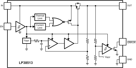
7.2 Functional Block Diagram

7.3 Feature Description
7.3.1 Short-Circuit Protection
The LP38513 is short-circuit protected and, in the event of a peak overcurrent condition, the short-circuit control loop rapidly drives the output PMOS pass element off. Once the power pass element shuts down, the control loop rapidly cycles the output on and off until the average power dissipation causes the thermal shutdown circuit to respond to servo the on/off cycling to a lower frequency. Refer to the Power Dissipation section for power dissipation calculations.
7.3.2 Enable
LP38513 has an EN pin to enable/disable the device. If the application does not require the enable function, the pin must be connected directly to the adjacent IN pin.
The status of the EN pin also affects the behavior of the ERROR flag. While the EN pin is high the regulator control loop is active, and the ERROR flag reorts the status of the output voltage. When the EN pin is taken low the regulator control loop is shut down, the output is turned off, and the internal logic immediately forces the ERROR flag pin low.
7.3.3 ERROR Flag
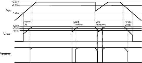
When the LP38513 EN pin is high, the ERROR flag pin produces a logic low signal when the output drops by more than 15% (VTH, typical) from the nominal output voltage. The drop in output voltage may be due to low input voltage, current limiting, or thermal limiting. This flag has a built-in hysteresis. The output voltage must to rise to greater than typically 89% of the nominal output voltage for the ERROR flag to return to a logic high state. Also, if the EN pin is pulled low, the ERROR flag pin is forced to low as well.
7.4 Device Functional Modes
7.4.1 Enable Operation
The Enable on/off threshold is typically 850 mV and has no hysteresis. The voltage signal must rise and fall cleanly, and promptly, through this threshold. The EN pin has no internal pullup or pulldown to establish a default condition and, as a result, this pin must be terminated either actively or passively.
If the EN pin is driven from a single ended device (such as the collector of a discrete transistor) a pullup resistor to VIN, or a pulldown resistor to ground, is required for proper operation. A 1-kΩ to 100-kΩ resistor can be used as the pullup or pulldown resistor to establish default condition for the EN pin. The resistor value selected must be appropriate to swamp out any leakage in the external single-ended device, as well as any stray capacitance.
If the EN pin is driven from a source that actively pulls high and low (such as a CMOS rail-to-rail comparator output), the pullup or pulldown resistor is not required.
If the application does not require the enable function, the EN pin must be connected directly to the adjacent IN pin.
7.4.2 ERROR Flag Operation
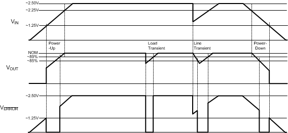
The internal ERROR flag comparator has an open-drain output stage. Hence, the ERROR pin requires an external pullup resistor. The value of the pullup resistor must be in the range of 2 kΩ to 20 kΩ and must be connected to the LP38513 OUT pin. The ERROR flag pin must not be pulled up to any voltage source higher than VIN as current flow through an internal parasitic diode may cause unexpected behavior. When the input voltage is less than typically 1.25 V the status of the ERROR flag output is not reliable. The ERROR flag pin must be connected to ground if this function is not used.
The timing diagram in Figure 16 shows the relationship between the ERROR flag and the output voltage when a pullup resistor is connected to the output voltage pin.
The timing diagram in Figure 17 shows the relationship between the ERROR flag and the output voltage when the pullup resistor is connected to the input voltage.
 Figure 16. ERROR Flag Operation (see Figure 18)
 Figure 17. ERROR Flag Operation Biased from VIN