ZHCSHM1C September 2017 – March 2018 LMZM33603
PRODUCTION DATA.
- 1 特性
- 2 应用
- 3 说明
- 4 修订历史记录
- 5 Pin Configuration and Functions
- 6 Specifications
-
7 Detailed Description
- 7.1 Overview
- 7.2 Functional Block Diagram
- 7.3
Feature Description
- 7.3.1 Adjusting the Output Voltage
- 7.3.2 Feed-Forward Capacitor, CFF
- 7.3.3 Output Current vs Output Voltage
- 7.3.4 Voltage Dropout
- 7.3.5 Switching Frequency (RT)
- 7.3.6 Synchronization (SYNC)
- 7.3.7 Input Capacitors
- 7.3.8 Output Capacitors
- 7.3.9 Output On/Off Enable (EN)
- 7.3.10 Programmable Undervoltage Lockout (UVLO)
- 7.3.11 Power Good (PGOOD)
- 7.3.12 Overcurrent Protection (OCP)
- 7.3.13 Thermal Shutdown
- 7.4 Device Functional Modes
- 8 Application and Implementation
- 9 Power Supply Recommendations
- 10Layout
- 11器件和文档支持
- 12机械、封装和可订购信息
7.3.9 Output On/Off Enable (EN)
The voltage on the EN/SYNC pin provides electrical ON/OFF control of the device. Once the EN pin voltage exceeds the threshold voltage, the device starts operation. If the EN pin voltage is pulled below the threshold voltage, the regulator stops switching and enters low quiescent current state.
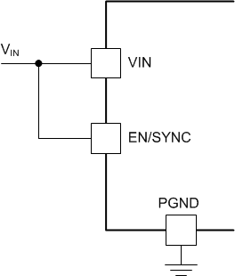
The EN pin cannot be open circuit or floating. The simplest way to enable the operation of the LMZM33603 is to connect the EN pin to VIN directly as shown in Figure 27. This allows self-start-up of the LMZM33603 when VIN is within the operation range.
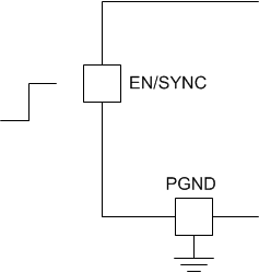
If an application requires controlling the EN pin, an external logic signal can be used to drive EN/SYNC pin as shown in Figure 28. Applications using an open drain/collector device to interface with this pin require a pullup resistor to a voltage above the enable threshold.
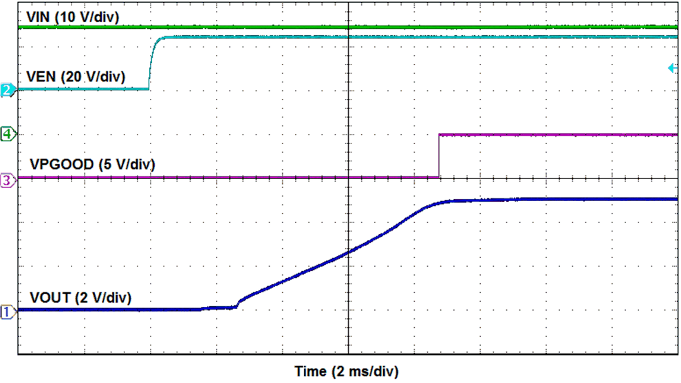
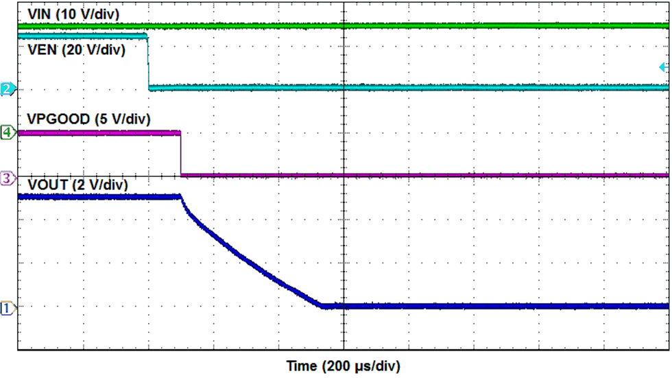
Figure 29 and Figure 30 show typical turn-ON and turn-OFF waveforms using the enable control.
 Figure 27. Enabling the Device
 Figure 28. Typical Enable Control
 Figure 29. Enable Turn-ON
 Figure 30. Enable Turn-OFF