ZHCSHM1C September 2017 – March 2018 LMZM33603
PRODUCTION DATA.
- 1 特性
- 2 应用
- 3 说明
- 4 修订历史记录
- 5 Pin Configuration and Functions
- 6 Specifications
-
7 Detailed Description
- 7.1 Overview
- 7.2 Functional Block Diagram
- 7.3
Feature Description
- 7.3.1 Adjusting the Output Voltage
- 7.3.2 Feed-Forward Capacitor, CFF
- 7.3.3 Output Current vs Output Voltage
- 7.3.4 Voltage Dropout
- 7.3.5 Switching Frequency (RT)
- 7.3.6 Synchronization (SYNC)
- 7.3.7 Input Capacitors
- 7.3.8 Output Capacitors
- 7.3.9 Output On/Off Enable (EN)
- 7.3.10 Programmable Undervoltage Lockout (UVLO)
- 7.3.11 Power Good (PGOOD)
- 7.3.12 Overcurrent Protection (OCP)
- 7.3.13 Thermal Shutdown
- 7.4 Device Functional Modes
- 8 Application and Implementation
- 9 Power Supply Recommendations
- 10Layout
- 11器件和文档支持
- 12机械、封装和可订购信息
7.3.4 Voltage Dropout
Voltage dropout is the difference between the input voltage and output voltage that is required to maintain output voltage regulation while providing the rated output current.
To ensure the LMZM33603 maintains output voltage regulation at the recommended switching frequency, over the operating temperature range, the following requirements apply:
For output voltages ≤ 5 V, the minimum VIN is 4 V or (VOUT + 1.5 V), whichever is greater.
For output voltages > 5 V, the minimum VIN is (1.3 × VOUT).
space
However, if fixed switching frequency operation is not required, the LMZM33603 operates in a frequency foldback mode when the dropout voltage is less than the recommendations above. Frequency foldback reduces the switching frequency to allow the output voltage to maintain regulation as input voltage decreases. Figure 20 through Figure 25 show typical dropout voltage and frequency foldback curves for 3.3 V, 5 V, and 12 V outputs at TA = 25°C. (Note: As ambient temperature increases, dropout voltage and frequency foldback occur at higher input voltage.)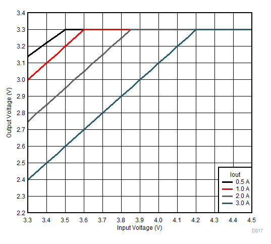
| VOUT = 3.3 V | fSW = 300 kHz |
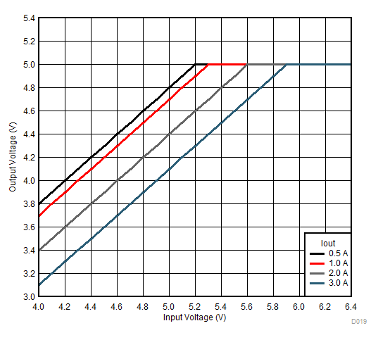
| VOUT = 5 V | fSW = 450 kHz |
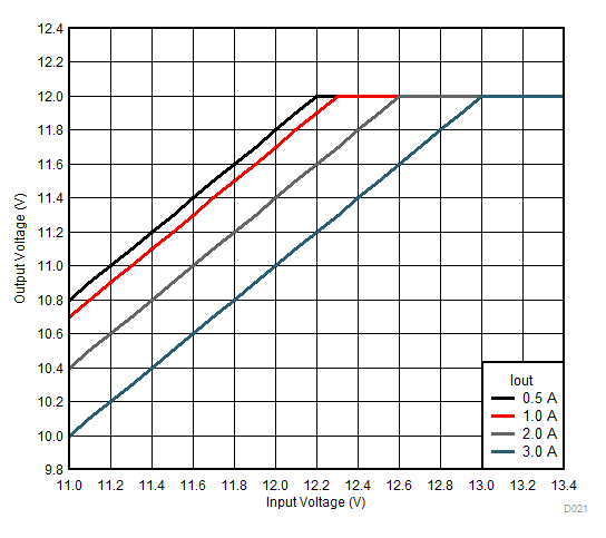
| VOUT = 12 V | fSW = 900 kHz |
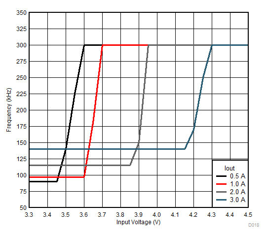
| VOUT = 3.3 V | fSW = 300 kHz |
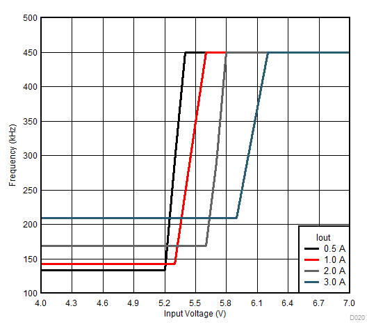
| VOUT = 5 V | fSW = 450 kHz |
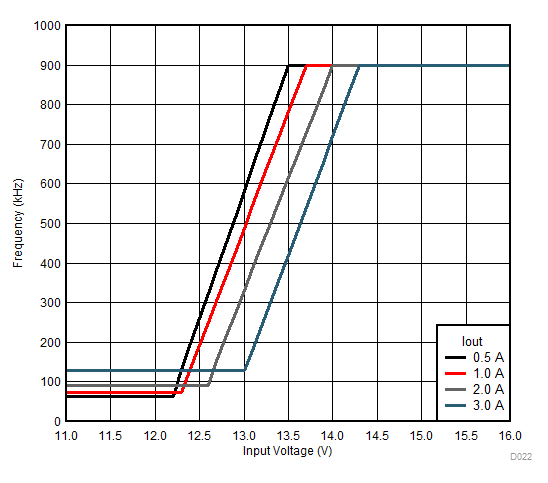
| VOUT = 12 V | fSW = 900 kHz |