ZHCSD96G August 2012 – September 2014 LMX2581
PRODUCTION DATA.
- 1 特性
- 2 应用
- 3 说明
- 4 简化电路原理图
- 5 修订历史记录
- 6 Pin Configuration and Functions
- 7 Specifications
-
8 Detailed Description
- 8.1 Overview
- 8.2 Functional Block Diagram
- 8.3
Feature Description
- 8.3.1 Typical Performance Characteristics
- 8.3.2 Impact of Temperature on VCO Phase Noise
- 8.3.3 OSCin INPUT and OSCin Doubler
- 8.3.4 R Divider
- 8.3.5 PLL N Divider And Fractional Circuitry
- 8.3.6 PLL Phase Detector and Charge Pump
- 8.3.7 External Loop Filter
- 8.3.8 Low Noise, Fully Integrated VCO
- 8.3.9 Programmable VCO Divider
- 8.3.10 0-Delay Mode
- 8.3.11 Programmable RF Output Buffers
- 8.3.12 Fastlock
- 8.3.13 Lock Detect
- 8.3.14 Part ID and Register Readback
- 8.3.15 Optimization of Spurs
- 8.4 Device Functional Modes
- 8.5 Programming
- 8.6
Register Maps
- 8.6.1
Programming Word Descriptions
- 8.6.1.1 Register R15
- 8.6.1.2 Register R13
- 8.6.1.3 Registers R10, R9, and R8
- 8.6.1.4 Register R7
- 8.6.1.5 Register R6
- 8.6.1.6
Register R5
- 8.6.1.6.1 OUT_LDEN — Mute Outputs Based on Lock Detect
- 8.6.1.6.2 OSC_FREQ[2:0] — OSCin Frequency for VCO Calibration
- 8.6.1.6.3 BUFEN_DIS - Disable for the BUFEN Pin
- 8.6.1.6.4 VCO_SEL_MODE — Method of Selecting Internal VCO Core
- 8.6.1.6.5 OUTB_MUX — Mux for RFoutB
- 8.6.1.6.6 OUTA_MUX — Mux for RFoutA
- 8.6.1.6.7 0_DLY - Zero Delay Mode
- 8.6.1.6.8 MODE[1:0] — Operating Mode
- 8.6.1.6.9 PWDN_MODE - Powerdown Mode
- 8.6.1.6.10 RESET - Register Reset
- 8.6.1.7 Register R4
- 8.6.1.8 Register R3
- 8.6.1.9 Register R2
- 8.6.1.10 Register R1
- 8.6.1.11 Register R0
- 8.6.1
Programming Word Descriptions
- 9 Application and Implementation
- 10Power Supply Recommendations
- 11Layout
- 12器件和文档支持
- 13机械封装和可订购信息
7 Specifications
7.1 Absolute Maximum Ratings(1)
over operating free-air temperature range (unless otherwise noted)| MIN | MAX | UNIT | ||
|---|---|---|---|---|
| Vcc | Power Supply Voltage | -0.3 | 3.6 | V |
| VIN | Input Voltage to Pins other than Vcc Pins | -0.3 | (Vcc + 0.3) | V |
| TL | Lead Temperature (solder 4 sec.) | +260 | °C | |
| TJ | Junction Temperature | +150 | °C | |
| VOSCin | Voltage on OSCin (Pin29) | ≤1.8 with Vcc Applied ≤1 with Vcc=0 |
Vpp | |
(1) Stresses beyond those listed under Absolute Maximum Ratings may cause permanent damage to the device. These are stress ratings only, which do not imply functional operation of the device at these or any other conditions beyond those indicated under Recommended Operating Conditions. Exposure to absolute-maximum-rated conditions for extended periods may affect device reliability.
7.2 Handling Ratings(1)
| MIN | MAX | UNIT | |||
|---|---|---|---|---|---|
| TSTG | Storage Temperature Range | -65 | 150 | °C | |
| VESD | Electrostatic Discharge | Human body model (HBM), per ANSI/ESDA/JEDEC JS-001, all pins(2) | 2500 | V | |
| Charged device model (CDM), per JEDEC specification JESD22-C101, all pins(3) | 1250 | ||||
| Machine Model (MM)(4) | 250 | ||||
(1) This device should only be assembled in ESD free workstations.
(2) JEDEC document JEP155 states that 2500-V HBM allows safe manufacturing with a standard ESD control process.
(3) JEDEC document JEP157 states that 1250-V CDM allows safe manufacturing with a standard ESD control process.
(4) JEDEC document JEP157 states that 250-V MM allows safe manufacturing with a standard ESD control process.
7.3 Recommended Operating Conditions
over operating free-air temperature range (unless otherwise noted)| MIN | TYP | MAX | UNIT | ||
|---|---|---|---|---|---|
| Vcc | Power Supply Voltage | 3.15 | 3.3 | 3.45 | V |
| TJ | Junction Temperature | 125 | °C | ||
| TA | Ambient Temperature | -40 | 85 | °C |
7.4 Thermal Information
| THERMAL METRIC(1) | DAP 32 PINS |
UNIT | |
|---|---|---|---|
| RθJA | Junction-to-ambient thermal resistance | 30 | °C/W |
| RθJC(bot) | Junction-to-case (bottom) thermal resistance | 4 | |
(1) For more information about traditional and new thermal metrics, see the IC Package Thermal Metrics application report, SPRA953.
7.5 Electrical Characteristics
(3.15 V ≤ Vcc ≤ 3.45 V, -40°C ≤ TA ≤ 85 °C; except as specified. Typical values are at Vcc = 3.3 V, 25 °C.)| PARAMETER | TEST CONDITIONS | MIN | TYP | MAX | UNIT | ||||
|---|---|---|---|---|---|---|---|---|---|
| CURRENT CONSUMPTION | |||||||||
| ICC | Entire Chip Supply Current | One Output Enabled OUTx_PWR = 15 |
178 | mA | |||||
| ICCCore | Supply Current Except for Output Buffers | Output Buffers and VCO Divider Disabled. | 134 | mA | |||||
| ICCRFout | Additive Current for EachOutput Buffer | OUTx_PWR = 15 | 44 | mA | |||||
| ICCVCO_DIV | Additive VCO Divider Current | VCO Divider Enabled | 20 | mA | |||||
| ICCPD | Power Down Current | Device Powered Down (CE Pin = LOW) |
7 | mA | |||||
| OSCin REFERENCE INPUT | |||||||||
| fOSCin | OSCin Frequency Range | Doubler Enabled | 5 | 250 | MHz | ||||
| Doubler Disabled | 5 | 900 | |||||||
| vOSCin | OSCin Input Voltage | AC Coupled | 0.4 | 1.7 | Vpp | ||||
| SpurFoscin | Oscin Spur | Foscin = 100 MHz, Offset = 100 MHz | -81 | dBc | |||||
| PLL | |||||||||
| fPD | Phase Detector Frequency | 200 | MHz | ||||||
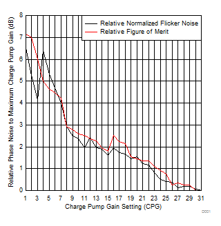
| KPD | Charge Pump Gain | Gain = 1X | 110 | µA | |||||
| Gain = 2X | 220 | ||||||||
| ... | ... | ||||||||
| Gain = 31X | 3410 | ||||||||
| PNPLL_1/f_Norm | Normalized PLL 1/f Noise (1) |
Gain =31X Normalized to 1 GHz carrier and 10 kHz Offset |
–120.8 | dBc /Hz | |||||
| PNPLL_FOM | PLL Figure of Merit (Normalized Noise Floor) (1) |
Gain =31X.
Normalized to PLL1 and fPD=1Hz |
–229 | dBc /Hz | |||||
| fRFin | External VCO Input Pin Frequency | Internal VCOs Bypassed (OUTA_PD=OUTB_PD=1) |
0.5 | 2.2 | GHz | ||||
| pRFin | External VCO Input Pin Power | Internal VCOs Bypassed (OUTA_PD=OUTB_PD=1) |
0 | +8 | dBm | ||||
| SpurFpd | Phase Detector Spurs (2) |
Fpd = 25 MHz | –85 | dBc | |||||
| Fpd = 100 MHz | –81 | ||||||||
| OUTPUTS | |||||||||
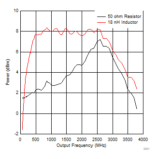
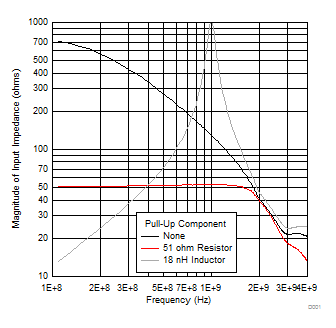
| pRFoutA+/-
pRFoutB+/- |
Output Power Level(5)(5) | Inductor Pull-Up Fout=2.7 GHz |
OUTx_PWR=15 | 7.3 | dBm | ||||
| OUTx_PWR=45 | 12 | ||||||||
| H2RFoutX+/- | Second Harmonic (6) |
Fout = 2.7 GHz | OUTx_PWR=15 | –25 | dBc | ||||
| VCO | |||||||||
| fVCO | Before the VCO Divider | All VCO Cores Combined | 1880 | 3760 | |||||
| KVCO | VCO Gain | Vtune = 1.3 Volts |
Core 1 | 12 to 24 | MHz/V | ||||
| Core 2 | 15 to 30 | ||||||||
| Core 3 | 20 to 37 | ||||||||
| Core 4 | 21 to 37 | ||||||||
| ΔTCL | Allowable Temperature Drift (3) |
VCO not being recalibrated | Fvco ≥2.5 GHz | –125 | +125 | °C | |||
| Fvco < 2.5 GHz | –100 | +125 | |||||||
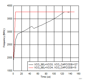
| tVCOCal | VCO Calibration Time (4) |
fOSCin = 100 MHz fPD = 100 MHz Full Band Change 1880 — 3760 MHz |
No Pre-programming | 140 | us | ||||
| With Pre-programming | 10 | ||||||||
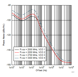
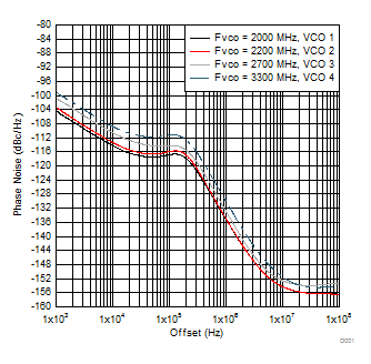
| PNVCO | VCO Phase Noise (OUTx_PWR =15) |
fVCO = 1.9 GHz Core 1 |
10 kHz Offset | –85.4 | dBc /Hz | ||||
| 100 kHz Offset | –114.5 | ||||||||
| 1 MHz Offset | –137.0 | ||||||||
| 10 MHz Offset | –154.2 | ||||||||
| 40 MHz Offset | –156.7 | ||||||||
| fVCO = 2.2 GHz Core 2 |
10 kHz Offset | –84.6 | dBc /Hz | ||||||
| 100 kHz Offset | –114.1 | ||||||||
| 1 MHz Offset | –137.5 | ||||||||
| 10 MHz Offset | –154.5 | ||||||||
| 40 MHz Offset | –156.1 | ||||||||
| fVCO = 2.7 GHz Core 3 |
10 kHz Offset | –81.7 | dBc /Hz | ||||||
| 100 kHz Offset | –112.2 | ||||||||
| 1 MHz Offset | –136.0 | ||||||||
| 10 MHz Offset | –153.1 | ||||||||
| 40 MHz Offset | –155.0 | ||||||||
| fVCO = 3.3 GHz Core 4 |
10 kHz Offset | –79.0 | dBc /Hz | ||||||
| 100 kHz Offset | –108.6 | ||||||||
| 1 MHz Offset | –132.6 | ||||||||
| 10 MHz Offset | –152.0 | ||||||||
| 40 MHz Offset | –155.0 | ||||||||
| DIGITAL INTERFACE (DATA, CLK, LE, CE, MUXout, BUFEN, LD) | |||||||||
| VIH | High-Level Input Voltage | 1.4 | Vcc | V | |||||
| VIL | Low Level Input Voltage | 0.4 | V | ||||||
| IIH | High-Level Input Current | VIH = 1.75 V | –5 | 5 | µA | ||||
| IIL | Low-Level Input Current | VIL = 0 V | –5 | 5 | µA | ||||
| VOH | High-Level Output Voltage | IOH = -500 µA | 2 | V | |||||
| VOL | Low-Level Output Voltage | IOL = -500 µA | 0 | 0.4 | V | ||||
(1) The PLL noise contribution is measured using a clean reference and a wide loop bandwidth and is composed into 1/f and flat components. PLL_Flat = PLL_FOM + 20*log(Fvco/Fpd)+10*log(Fpd / 1Hz). PLL_1/f = PLL_1/f_Norm + 20*log(Fvco / 1GHz) - 10*log(Offset/10kHz). Once these two components are found, the total PLL noise can be calculated as PLL_Noise = 10*log( 10PLL_Flat/10) + 10PLL_1/f / 10 )
(2) The spurs at the offset of the phase detector frequency are dependent on many factors, such as he phase detector frequency.
(3) Continuous tuning range over temperature refers to programming the device at an initial temperature and allowing this temperature to drift WITHOUT reprogramming the device. This change could be up or down in temperature and the specification does not apply to temperatures that go outside the recommended operating temperatures of the device.
(4) VCO digital calibration time is the amount of time it takes for the VCO to find the correct frequency band when switching to a new frequency. After the correct frequency band is found , the remaining error is typically less than 1 MHz and then the PLL settles the rest of the error in an analog manner. Pre-programming refers to specifying a band that is close to the final (<20 MHz), which greatly improves the VCO calibration time.
(5) The output power is dependent of the setup and is also programmable. Consult the Applications section for more information.
(6) The harmonics vary as a function of frequency, output termination, board layout, and output power setting.
7.6 Timing Requirements, MICROWIRE Timing
| MIN | TYP | MAX | UNIT | |||
|---|---|---|---|---|---|---|
| tES | Clock to Enable Low Time | See Figure 1 | 35 | ns | ||
| tCS | Data to Clock Set Up Time | See Figure 1 | 10 | ns | ||
| tCH | Data to Clock Hold Time | See Figure 1 | 10 | ns | ||
| tCWH | Clock Pulse Width High | See Figure 1 | 25 | ns | ||
| tCWL | Clock Pulse Width Low | See Figure 1 | 25 | ns | ||
| tCES | Enable to Clock Set Up Time | See Figure 1 | 10 | ns | ||
| tEWH | Enable Pulse Width High | See Figure 1 | 10 | ns |
 Figure 1. Serial Data Input Timing
7.7 Typical Characteristics