ZHCSD96G August   2012  – September 2014 LMX2581

PRODUCTION DATA.  

  1. 特性
  2. 应用
  3. 说明
  4. 简化电路原理图
  5. 修订历史记录
  6. Pin Configuration and Functions
  7. Specifications
    1. 7.1 Absolute Maximum Ratings
    2. 7.2 Handling Ratings
    3. 7.3 Recommended Operating Conditions
    4. 7.4 Thermal Information
    5. 7.5 Electrical Characteristics
    6. 7.6 Timing Requirements, MICROWIRE Timing
    7. 7.7 Typical Characteristics
  8. Detailed Description
    1. 8.1 Overview
    2. 8.2 Functional Block Diagram
    3. 8.3 Feature Description
      1. 8.3.1  Typical Performance Characteristics
        1. 8.3.1.1 Phase Noise Typical Performance Plot Explanations
        2. 8.3.1.2 Other Typical Performance Plot Characteristics Explanations
      2. 8.3.2  Impact of Temperature on VCO Phase Noise
      3. 8.3.3  OSCin INPUT and OSCin Doubler
      4. 8.3.4  R Divider
      5. 8.3.5  PLL N Divider And Fractional Circuitry
        1. 8.3.5.1 Programmable Dithering Levels
        2. 8.3.5.2 Programmable Delta Sigma Modulator Order
      6. 8.3.6  PLL Phase Detector and Charge Pump
      7. 8.3.7  External Loop Filter
      8. 8.3.8  Low Noise, Fully Integrated VCO
        1. 8.3.8.1 VCO Digital Calibration
      9. 8.3.9  Programmable VCO Divider
      10. 8.3.10 0-Delay Mode
      11. 8.3.11 Programmable RF Output Buffers
        1. 8.3.11.1 Choosing the Proper Pull-Up Component
        2. 8.3.11.2 Choosing the Best Setting for the RFoutA_PWR and RFoutB_PWR Words
      12. 8.3.12 Fastlock
      13. 8.3.13 Lock Detect
        1. 8.3.13.1 Vtune Lock Detect
        2. 8.3.13.2 Digital Lock Detect (DLD)
      14. 8.3.14 Part ID and Register Readback
        1. 8.3.14.1 Uses of Readback
        2. 8.3.14.2 Serial Timing for Readback
      15. 8.3.15 Optimization of Spurs
        1. 8.3.15.1 Phase Detector Spur
        2. 8.3.15.2 Fractional Spur - Integer Boundary Spur
        3. 8.3.15.3 Fractional Spur - Primary Fractional Spurs
        4. 8.3.15.4 Fractional Spur - Sub-Fractional Spurs
        5. 8.3.15.5 Summary of Spurs and Mitigation Techniques
    4. 8.4 Device Functional Modes
      1. 8.4.1 Full Synthesizer Mode
      2. 8.4.2 External VCO Mode
      3. 8.4.3 Powerdown Modes
    5. 8.5 Programming
      1. 8.5.1 Serial Data Input Timing
      2. 8.5.2 Recommended Initial Power on Programming Sequence
      3. 8.5.3 Recommended Sequence for Changing Frequencies
      4. 8.5.4 Triggering Registers
    6. 8.6 Register Maps
      1. 8.6.1 Programming Word Descriptions
        1. 8.6.1.1  Register R15
          1. 8.6.1.1.1 VCO_CAP_MAN — Manual VCO Band Select
          2. 8.6.1.1.2 VCO_CAPCODE[7:0] — Capacitor Value for VCO Band Selection
        2. 8.6.1.2  Register R13
          1. 8.6.1.2.1 DLD_ERR_CNT[3:0] - Digital Lock Detect Error Count
          2. 8.6.1.2.2 DLD_PASS_CNT[9:0] - Digital Lock Detect Success Count
          3. 8.6.1.2.3 DLD_TOL[2:0] — Digital Lock Detect
        3. 8.6.1.3  Registers R10, R9, and R8
        4. 8.6.1.4  Register R7
          1. 8.6.1.4.1 FL_PINMODE[2:0], MUXOUT_PINMODE[2:0], and LD_PINMODE[2:0] — Output Format for Status Pins
          2. 8.6.1.4.2 FL_INV, MUX_INV, LD_INV - Inversion for Status Pins
          3. 8.6.1.4.3 FL_SELECT[4:0], MUXOUT_SELECT[4:0], LD_SELECT[4:0] — State for Status Pins
        5. 8.6.1.5  Register R6
          1. 8.6.1.5.1 RD_DIAGNOSTICS[19:0] — Readback Diagnostics
          2. 8.6.1.5.2 RDADDR[3:0] — Readback Address
          3. 8.6.1.5.3 uWIRE_LOCK - Microwire lock
        6. 8.6.1.6  Register R5
          1. 8.6.1.6.1  OUT_LDEN — Mute Outputs Based on Lock Detect
          2. 8.6.1.6.2  OSC_FREQ[2:0] — OSCin Frequency for VCO Calibration
          3. 8.6.1.6.3  BUFEN_DIS - Disable for the BUFEN Pin
          4. 8.6.1.6.4  VCO_SEL_MODE — Method of Selecting Internal VCO Core
          5. 8.6.1.6.5  OUTB_MUX — Mux for RFoutB
          6. 8.6.1.6.6  OUTA_MUX — Mux for RFoutA
          7. 8.6.1.6.7  0_DLY - Zero Delay Mode
          8. 8.6.1.6.8  MODE[1:0] — Operating Mode
          9. 8.6.1.6.9  PWDN_MODE - Powerdown Mode
          10. 8.6.1.6.10 RESET - Register Reset
        7. 8.6.1.7  Register R4
          1. 8.6.1.7.1 PFD_DLY[2:0] — Phase Detector Delay
          2. 8.6.1.7.2 FL_FRCE — Force Fastlock Conditions
          3. 8.6.1.7.3 FL_TOC[11:0] — Fastlock Timeout Counter
          4. 8.6.1.7.4 FL_CPG[4:0] — Fastlock Charge Pump Gain
          5. 8.6.1.7.5 CPG_BLEED[5:0]
        8. 8.6.1.8  Register R3
          1. 8.6.1.8.1 VCO_DIV[4:0] — VCO Divider Value
          2. 8.6.1.8.2 OUTB_PWR[5:0] — RFoutB Output Power
          3. 8.6.1.8.3 OUTA_PWR[5:0] — RFoutA Output Power
          4. 8.6.1.8.4 OUTB_PD — RFoutB Powerdown
          5. 8.6.1.8.5 OUTA_PD — RFoutA Powerdown
        9. 8.6.1.9  Register R2
          1. 8.6.1.9.1 OSC_2X — OSCin Doubler
          2. 8.6.1.9.2 CPP - Charge Pump Polarity
          3. 8.6.1.9.3 PLL_DEN[21:0] — PLL Fractional Denominator
        10. 8.6.1.10 Register R1
          1. 8.6.1.10.1 CPG[4:0] — PLL Charge Pump Gain
          2. 8.6.1.10.2 VCO_SEL[1:0] - VCO Selection
          3. 8.6.1.10.3 FRAC_ORDER[2:0] — PLL Delta Sigma Modulator Order
          4. 8.6.1.10.4 PLL_R[7:0] — PLL R divider
        11. 8.6.1.11 Register R0
          1. 8.6.1.11.1 ID - Part ID Readback
          2. 8.6.1.11.2 FRAC_DITHER[1:0] — PLL Fractional Dithering
          3. 8.6.1.11.3 NO_FCAL — Disable Frequency Calibration
          4. 8.6.1.11.4 PLL_N - PLL Feedback Divider Value
          5. 8.6.1.11.5 PLL_NUM[21:12] and PLL_NUM[11:0] — PLL Fractional Numerator
  9. Application and Implementation
    1. 9.1 Application Information
    2. 9.2 Typical Applications
      1. 9.2.1 Clocking Application
        1. 9.2.1.1 Design Requirements
        2. 9.2.1.2 Detailed Design Procedure
        3. 9.2.1.3 Application Curves
      2. 9.2.2 Fractional PLL Application
        1. 9.2.2.1 Design Requirements
        2. 9.2.2.2 Detailed Design Procedure
        3. 9.2.2.3 Application Curves
    3. 9.3 Do's and Don'ts
  10. 10Power Supply Recommendations
    1. 10.1 Supply Recommendations
    2. 10.2 Regulator Output Pins
  11. 11Layout
    1. 11.1 Layout Guidelines
    2. 11.2 Layout Example
  12. 12器件和文档支持
    1. 12.1 器件支持
    2. 12.2 文档支持
      1. 12.2.1 相关文档 
    3. 12.3 商标
    4. 12.4 静电放电警告
    5. 12.5 术语表
  13. 13机械封装和可订购信息

封装选项

机械数据 (封装 | 引脚)
散热焊盘机械数据 (封装 | 引脚)
订购信息

10 Power Supply Recommendations

10.1 Supply Recommendations

Low noise regulators are generally recommended for the supply pins. It is OK to have one regulator supply the part, although it is best to put individual bypassing as shown in the Layout Guidelines for the best spur performance. The most noise sensitive components are the pull-up components for the output buffers since supply noise here will directly go to the output. For purposes of bypassing, below is how the current consumption is approximately distributed through each pin. For this table, default mode is with internal VCO mode with one output buffer powered up with OUTx_PWR=15. External VCO mode assumes the VCO divider and output buffers are off.

Table 16. Current Consumption by Pin

PIN NUMBER PIN NAME CONDITION
DEFAULT MODE DEFAULT MODE
with VCO DIVIDER ENABLED
EXTERNAL VCO MODE
with OUTPUT BUFFER DISABLED
Pin 6 VccCP 12 12 12
Pin 10 VccPLL 28 28 48
Pin 16 VccBUF 23 43 1
Pin 17 VccVCO 83 83 14
Pin 28 VccDIG 10 10 10
Pin 32 VccFRAC <<1 <<1 <<1
n/a Output Pull-Up Component 22 22 0
TOTAL 178 198 85

10.2 Regulator Output Pins

The recommendation for the VregVCO and VbiasCOMP pins is a minimum of one 10 µF capacitor, but more capacitance is better. These pins have a bias voltage of about 2.5 V, which means that capacitors of smaller case size and voltage ratings can actually have far less capacitance the labeled value of the capacitor. If there is insufficient capacitance on these pins, then the VCO phase noise may be degraded. This degradation may vary with frequency and how insufficient the capacitance is, but for example, bench tests show a degradation of about 5 dB at 20 KHz offset for a 3 GHz carrier if these capacitors are reduced to 4.7 µF.

ta_VregCap.gif
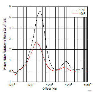
Figure 26. Impact of VregVCO and VbiasCOMP Capacitor on VCO Phase Noise