ZHCSD96G August   2012  – September 2014 LMX2581

PRODUCTION DATA.  

  1. 特性
  2. 应用
  3. 说明
  4. 简化电路原理图
  5. 修订历史记录
  6. Pin Configuration and Functions
  7. Specifications
    1. 7.1 Absolute Maximum Ratings
    2. 7.2 Handling Ratings
    3. 7.3 Recommended Operating Conditions
    4. 7.4 Thermal Information
    5. 7.5 Electrical Characteristics
    6. 7.6 Timing Requirements, MICROWIRE Timing
    7. 7.7 Typical Characteristics
  8. Detailed Description
    1. 8.1 Overview
    2. 8.2 Functional Block Diagram
    3. 8.3 Feature Description
      1. 8.3.1  Typical Performance Characteristics
        1. 8.3.1.1 Phase Noise Typical Performance Plot Explanations
        2. 8.3.1.2 Other Typical Performance Plot Characteristics Explanations
      2. 8.3.2  Impact of Temperature on VCO Phase Noise
      3. 8.3.3  OSCin INPUT and OSCin Doubler
      4. 8.3.4  R Divider
      5. 8.3.5  PLL N Divider And Fractional Circuitry
        1. 8.3.5.1 Programmable Dithering Levels
        2. 8.3.5.2 Programmable Delta Sigma Modulator Order
      6. 8.3.6  PLL Phase Detector and Charge Pump
      7. 8.3.7  External Loop Filter
      8. 8.3.8  Low Noise, Fully Integrated VCO
        1. 8.3.8.1 VCO Digital Calibration
      9. 8.3.9  Programmable VCO Divider
      10. 8.3.10 0-Delay Mode
      11. 8.3.11 Programmable RF Output Buffers
        1. 8.3.11.1 Choosing the Proper Pull-Up Component
        2. 8.3.11.2 Choosing the Best Setting for the RFoutA_PWR and RFoutB_PWR Words
      12. 8.3.12 Fastlock
      13. 8.3.13 Lock Detect
        1. 8.3.13.1 Vtune Lock Detect
        2. 8.3.13.2 Digital Lock Detect (DLD)
      14. 8.3.14 Part ID and Register Readback
        1. 8.3.14.1 Uses of Readback
        2. 8.3.14.2 Serial Timing for Readback
      15. 8.3.15 Optimization of Spurs
        1. 8.3.15.1 Phase Detector Spur
        2. 8.3.15.2 Fractional Spur - Integer Boundary Spur
        3. 8.3.15.3 Fractional Spur - Primary Fractional Spurs
        4. 8.3.15.4 Fractional Spur - Sub-Fractional Spurs
        5. 8.3.15.5 Summary of Spurs and Mitigation Techniques
    4. 8.4 Device Functional Modes
      1. 8.4.1 Full Synthesizer Mode
      2. 8.4.2 External VCO Mode
      3. 8.4.3 Powerdown Modes
    5. 8.5 Programming
      1. 8.5.1 Serial Data Input Timing
      2. 8.5.2 Recommended Initial Power on Programming Sequence
      3. 8.5.3 Recommended Sequence for Changing Frequencies
      4. 8.5.4 Triggering Registers
    6. 8.6 Register Maps
      1. 8.6.1 Programming Word Descriptions
        1. 8.6.1.1  Register R15
          1. 8.6.1.1.1 VCO_CAP_MAN — Manual VCO Band Select
          2. 8.6.1.1.2 VCO_CAPCODE[7:0] — Capacitor Value for VCO Band Selection
        2. 8.6.1.2  Register R13
          1. 8.6.1.2.1 DLD_ERR_CNT[3:0] - Digital Lock Detect Error Count
          2. 8.6.1.2.2 DLD_PASS_CNT[9:0] - Digital Lock Detect Success Count
          3. 8.6.1.2.3 DLD_TOL[2:0] — Digital Lock Detect
        3. 8.6.1.3  Registers R10, R9, and R8
        4. 8.6.1.4  Register R7
          1. 8.6.1.4.1 FL_PINMODE[2:0], MUXOUT_PINMODE[2:0], and LD_PINMODE[2:0] — Output Format for Status Pins
          2. 8.6.1.4.2 FL_INV, MUX_INV, LD_INV - Inversion for Status Pins
          3. 8.6.1.4.3 FL_SELECT[4:0], MUXOUT_SELECT[4:0], LD_SELECT[4:0] — State for Status Pins
        5. 8.6.1.5  Register R6
          1. 8.6.1.5.1 RD_DIAGNOSTICS[19:0] — Readback Diagnostics
          2. 8.6.1.5.2 RDADDR[3:0] — Readback Address
          3. 8.6.1.5.3 uWIRE_LOCK - Microwire lock
        6. 8.6.1.6  Register R5
          1. 8.6.1.6.1  OUT_LDEN — Mute Outputs Based on Lock Detect
          2. 8.6.1.6.2  OSC_FREQ[2:0] — OSCin Frequency for VCO Calibration
          3. 8.6.1.6.3  BUFEN_DIS - Disable for the BUFEN Pin
          4. 8.6.1.6.4  VCO_SEL_MODE — Method of Selecting Internal VCO Core
          5. 8.6.1.6.5  OUTB_MUX — Mux for RFoutB
          6. 8.6.1.6.6  OUTA_MUX — Mux for RFoutA
          7. 8.6.1.6.7  0_DLY - Zero Delay Mode
          8. 8.6.1.6.8  MODE[1:0] — Operating Mode
          9. 8.6.1.6.9  PWDN_MODE - Powerdown Mode
          10. 8.6.1.6.10 RESET - Register Reset
        7. 8.6.1.7  Register R4
          1. 8.6.1.7.1 PFD_DLY[2:0] — Phase Detector Delay
          2. 8.6.1.7.2 FL_FRCE — Force Fastlock Conditions
          3. 8.6.1.7.3 FL_TOC[11:0] — Fastlock Timeout Counter
          4. 8.6.1.7.4 FL_CPG[4:0] — Fastlock Charge Pump Gain
          5. 8.6.1.7.5 CPG_BLEED[5:0]
        8. 8.6.1.8  Register R3
          1. 8.6.1.8.1 VCO_DIV[4:0] — VCO Divider Value
          2. 8.6.1.8.2 OUTB_PWR[5:0] — RFoutB Output Power
          3. 8.6.1.8.3 OUTA_PWR[5:0] — RFoutA Output Power
          4. 8.6.1.8.4 OUTB_PD — RFoutB Powerdown
          5. 8.6.1.8.5 OUTA_PD — RFoutA Powerdown
        9. 8.6.1.9  Register R2
          1. 8.6.1.9.1 OSC_2X — OSCin Doubler
          2. 8.6.1.9.2 CPP - Charge Pump Polarity
          3. 8.6.1.9.3 PLL_DEN[21:0] — PLL Fractional Denominator
        10. 8.6.1.10 Register R1
          1. 8.6.1.10.1 CPG[4:0] — PLL Charge Pump Gain
          2. 8.6.1.10.2 VCO_SEL[1:0] - VCO Selection
          3. 8.6.1.10.3 FRAC_ORDER[2:0] — PLL Delta Sigma Modulator Order
          4. 8.6.1.10.4 PLL_R[7:0] — PLL R divider
        11. 8.6.1.11 Register R0
          1. 8.6.1.11.1 ID - Part ID Readback
          2. 8.6.1.11.2 FRAC_DITHER[1:0] — PLL Fractional Dithering
          3. 8.6.1.11.3 NO_FCAL — Disable Frequency Calibration
          4. 8.6.1.11.4 PLL_N - PLL Feedback Divider Value
          5. 8.6.1.11.5 PLL_NUM[21:12] and PLL_NUM[11:0] — PLL Fractional Numerator
  9. Application and Implementation
    1. 9.1 Application Information
    2. 9.2 Typical Applications
      1. 9.2.1 Clocking Application
        1. 9.2.1.1 Design Requirements
        2. 9.2.1.2 Detailed Design Procedure
        3. 9.2.1.3 Application Curves
      2. 9.2.2 Fractional PLL Application
        1. 9.2.2.1 Design Requirements
        2. 9.2.2.2 Detailed Design Procedure
        3. 9.2.2.3 Application Curves
    3. 9.3 Do's and Don'ts
  10. 10Power Supply Recommendations
    1. 10.1 Supply Recommendations
    2. 10.2 Regulator Output Pins
  11. 11Layout
    1. 11.1 Layout Guidelines
    2. 11.2 Layout Example
  12. 12器件和文档支持
    1. 12.1 器件支持
    2. 12.2 文档支持
      1. 12.2.1 相关文档 
    3. 12.3 商标
    4. 12.4 静电放电警告
    5. 12.5 术语表
  13. 13机械封装和可订购信息

封装选项

机械数据 (封装 | 引脚)
散热焊盘机械数据 (封装 | 引脚)
订购信息

11 Layout

11.1 Layout Guidelines

For the Layout of the LMX2581, the pull-up component for the output buffers should be as close to the chip as possible in order to get the most possible output power.

The following layout guidelines apply. The designators match those shown in the applications schematic.

  1. RFoutA & B Pull-Up Components: The pull-up components are close. If using only one output, these components can be made even closer for an improvement in output power
  2. Ground for VbiasVCO and VbiasCOMP: There is a solid connection for the ground between the VbiasVCO and VbiasCOMP pins and pin 18. This minimizes the VCO phase noise.
  3. Loop Filter: One loop filter capacitor is next to the VCO. The charge pump output and Vtune input are on opposite sides of the chip. Although one can not get the whole loop filter close to the chip without compromising the grounding for the VbiasVCO and VbiasCOMP pins, it is possible to get the highest order loop filter capacitor there. Also, for the vias used, keep the ground plane far away so it does not couple spur energy into the VCO input.

11.2 Layout Example

pcb_snas601.png
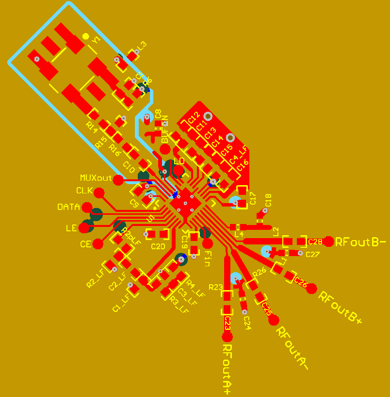
Figure 27. LMX2581 Layout Example