ZHCSM75V August 1999 – May 2025 LMV331 , LMV339 , LMV393
PRODUCTION DATA
- 1
- 1 特性
- 2 应用
- 3 说明
- 4 Pin Configuration and Functions
-
5 Specifications
- 5.1 Absolute Maximum Ratings
- 5.2 ESD Ratings
- 5.3 Recommended Operating Conditions
- 5.4 Thermal Information
- 5.5 Electrical Characteristics, VCC+ = 2.7V
- 5.6 Switching Characteristics, VCC+ = 2.7V
- 5.7 Electrical Characteristics, VCC+ = 5V
- 5.8 Switching Characteristics, VCC+ = 5V
- 5.9 Typical Characteristics
- 6 Detailed Description
- 7 Application and Implementation
- 8 Power Supply Recommendations
- 9 Layout
- 10Device and Documentation Support
- 11Trademarks
- 12静电放电警告
- 13术语表
- 14Revision History
- 15Mechanical, Packaging, and Orderable Information
封装选项
请参考 PDF 数据表获取器件具体的封装图。
机械数据 (封装 | 引脚)
- D|14
- PW|14
散热焊盘机械数据 (封装 | 引脚)
订购信息
5.9 Typical Characteristics
Unless otherwise specified, VS = +5V, single supply, TA = 25°C
 Figure 5-1 Supply Current vs Supply Voltage Output High
 Figure 5-3 Output Voltage vs Output Current
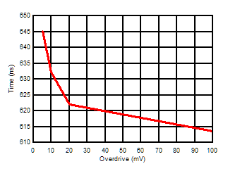
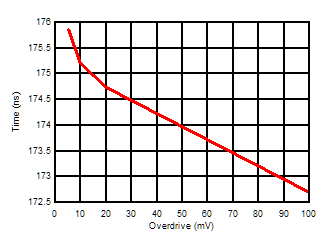
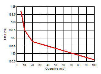
 Figure 5-5 Response Time vs Input Overdrives Negative Transition (VCC=5V)
 Figure 5-7 Response Time vs Input Overdrives Negative Transition (VCC = 2.7V)
 Figure 5-2 Supply Current vs Supply Voltage Output Low
 Figure 5-4 Input Bias Current vs Supply Voltage
 Figure 5-6 Response Time vs Input Overdrives Positive Transition (VCC = 5V)
 Figure 5-8 Response Time vs Input Overdrives Positive Transition (VCC = 2.7V)