ZHCSIN5D August 2018 – August 2022 LMR36006-Q1
PRODUCTION DATA
- 1 特性
- 2 应用
- 3 说明
- 4 Revision History
- 5 Device Comparison Table
- 6 Pin Configuration and Functions
- 7 Specifications
- 8 Detailed Description
-
9 Application and Implementation
- 9.1 Application Information
- 9.2
Typical Application
- 9.2.1
Design 1: Low Power 24-V, 600-mA PFM Converter
- 9.2.1.1 Design Requirements
- 9.2.1.2
Detailed Design Procedure
- 9.2.1.2.1 Custom Design With WEBENCH Tools
- 9.2.1.2.2 Choosing the Switching Frequency
- 9.2.1.2.3 Setting the Output Voltage
- 9.2.1.2.4 Inductor Selection
- 9.2.1.2.5 Output Capacitor Selection
- 9.2.1.2.6 Input Capacitor Selection
- 9.2.1.2.7 CBOOT
- 9.2.1.2.8 VCC
- 9.2.1.2.9 CFF Selection
- 9.2.1.2.10 Maximum Ambient Temperature
- 9.2.1.3 Application Curves
- 9.2.2 Design 2: High Density 12-V , 600-mA FPWM Converter
- 9.2.1
Design 1: Low Power 24-V, 600-mA PFM Converter
- 9.3 What to Do and What Not to Do
- 10Power Supply Recommendations
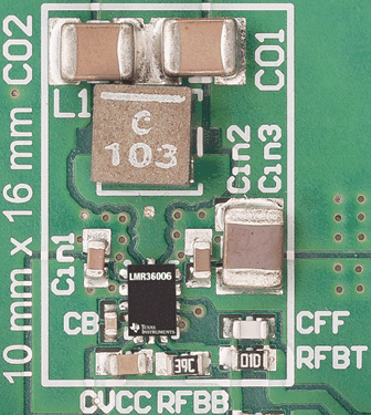
- 11Layout
- 12Device and Documentation Support
- 13Mechanical, Packaging, and Orderable Information
3 说明
LMR36006-Q1 稳压器是一款易于使用的同步降压直流/直流转换器。该器件具有集成式高侧和低侧功率 MOSFET,能够提供高达 0.6A 的输出电流(在 4.2V 至 60V 的宽输入电压范围内)。容差高达 66V。
LMR36006-Q1 采用峰值电流模式控制机制来提供最佳的效率和输出电压精度。LMR36006-Q1 可利用高级高速电路在 2.1MHz 的固定频率下实现从 20V 输入到 5V 输出的稳压。精密使能支持直接连接到宽输入电压或对器件启动和关断进行精确控制,因此提供了灵活性。附带内置滤波和延迟功能的电源正常状态标志可提供系统状态的真实指示,免去了使用外部监测器的麻烦。
LMR36006-Q1 采用 HotRod™ 封装,实现了低 EMI、更高的效率和超小的封装裸片比。此器件需要很少的外部元件,并且具有可简化 PCB 布局的引脚排列。LMR36006-Q1 的小型解决方案尺寸和各种功能旨在简化各种终端设备的实现。
器件信息
| 器件型号 | 封装(1) | 封装尺寸(标称值) |
|---|---|---|
| LMR36006-Q1 | VQFN-HR (12) | 2.00mm x 3.00mm |
(1) 如需了解所有可用封装,请参阅数据表末尾的可订购产品附录。
 简化版原理图