ZHCSJY0B June   2012  – June 2019 LMR12015 , LMR12020

PRODUCTION DATA.  

  1. 特性
  2. 应用
  3. 说明
    1.     Device Images
      1.      典型应用电路
  4. 修订历史记录
  5. Pin Configuration and Functions
    1.     Pin Descriptions
  6. Specifications
    1. 6.1 Absolute Maximum Ratings
    2. 6.2 Recommended Operating Ratings
    3. 6.3 Electrical Characteristics
    4. 6.4 Typical Performance Characteristics
  7. Detailed Description
    1. 7.1 Overview
    2. 7.2 Functional Block Diagram
    3. 7.3 Feature Description
      1. 7.3.1  Boost Function
      2. 7.3.2  Low Input Voltage Considerations
      3. 7.3.3  High Output Voltage Considerations
      4. 7.3.4  Frequency Synchronization
      5. 7.3.5  Current Limit
      6. 7.3.6  Frequency Foldback
      7. 7.3.7  Soft Start
      8. 7.3.8  Output Overvoltage Protection
      9. 7.3.9  Undervoltage Lockout
      10. 7.3.10 Thermal Shutdown
    4. 7.4 Device Operation Modes
      1. 7.4.1 Enable Pin / Shutdown Mode
  8. Application and Implementation
    1. 8.1 Application Information
    2. 8.2 Typical Application
      1. 8.2.1 Detailed Design Procedure
        1. 8.2.1.1  Custom Design With WEBENCH® Tools
        2. 8.2.1.2  Inductor Selection
          1. 8.2.1.2.1 Inductor Calculation Example
          2. 8.2.1.2.2 Inductor Material Selection
        3. 8.2.1.3  Input Capacitor
        4. 8.2.1.4  Output Capacitor
        5. 8.2.1.5  Catch Diode
        6. 8.2.1.6  Boost Diode (Optional)
        7. 8.2.1.7  Boost Capacitor
        8. 8.2.1.8  Output Voltage
        9. 8.2.1.9  Feedforward Capacitor (Optional)
        10. 8.2.1.10 Calculating Efficiency and Junction Temperature
          1. 8.2.1.10.1 Schottky Diode Conduction Losses
          2. 8.2.1.10.2 Inductor Conduction Losses
          3. 8.2.1.10.3 MOSFET Conduction Losses
          4. 8.2.1.10.4 MOSFET Switching Losses
          5. 8.2.1.10.5 IC Quiescent Losses
          6. 8.2.1.10.6 MOSFET Driver Losses
          7. 8.2.1.10.7 Total Power Losses
          8. 8.2.1.10.8 Efficiency Calculation Example
          9. 8.2.1.10.9 Calculating the LMR2015/20 Junction Temperature
      2. 8.2.2 Application Curves
      3. 8.2.3 LMR12015/20 Circuit Examples
  9. Layout
    1. 9.1 Layout Considerations
      1. 9.1.1 Compact Layout
      2. 9.1.2 Ground Plane and Shape Routing
      3. 9.1.3 FB Loop
      4. 9.1.4 PCB Summary
  10. 10器件和文档支持
    1. 10.1 器件支持
      1. 10.1.1 第三方产品免责声明
      2. 10.1.2 开发支持
        1. 10.1.2.1 使用 WEBENCH® 工具创建定制设计
    2. 10.2 相关链接
    3. 10.3 接收文档更新通知
    4. 10.4 社区资源
    5. 10.5 商标
    6. 10.6 静电放电警告
    7. 10.7 Glossary
  11. 11机械、封装和可订购信息

封装选项

机械数据 (封装 | 引脚)
散热焊盘机械数据 (封装 | 引脚)
订购信息

Application Curves

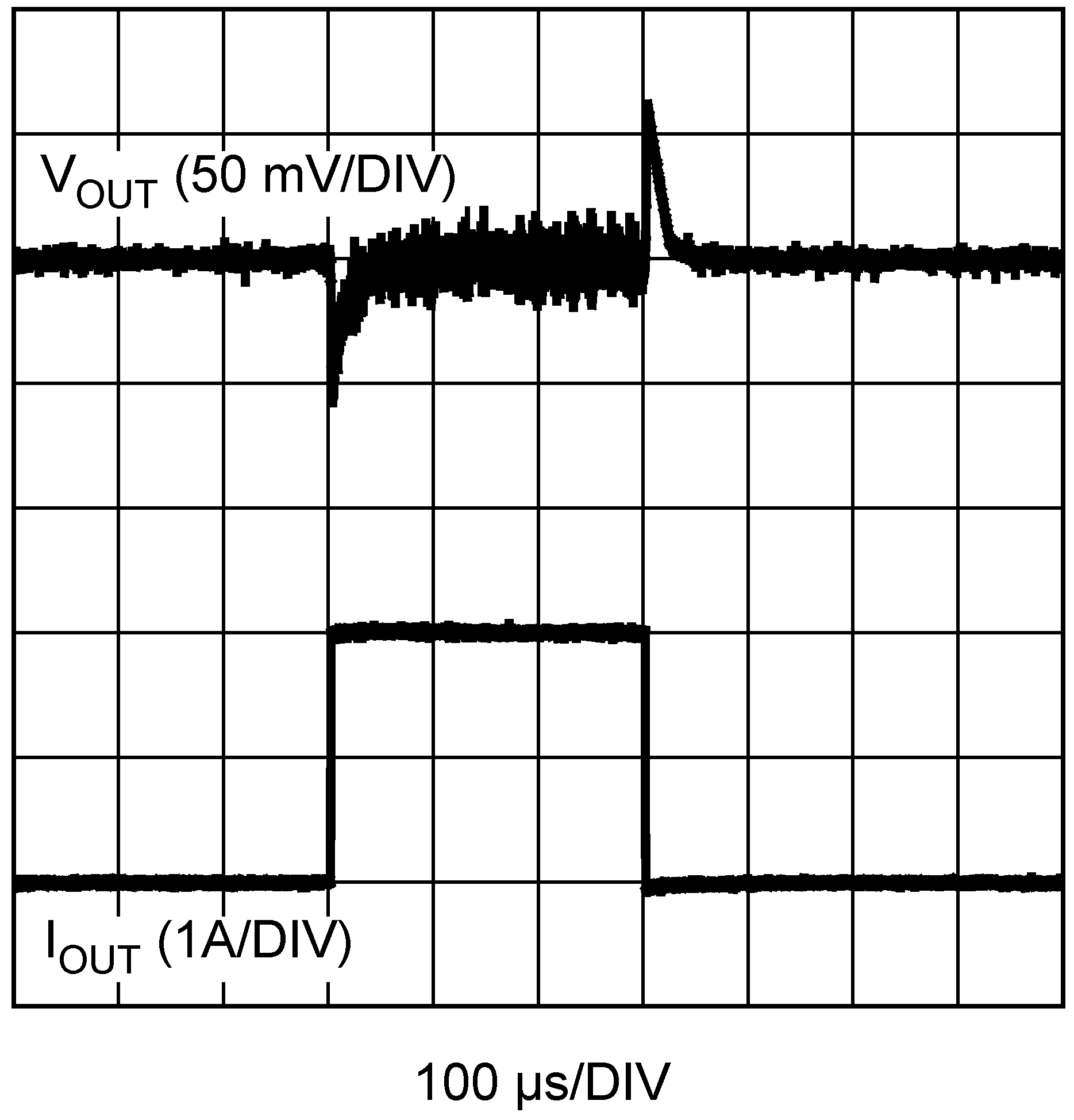
LMR12015 LMR12020 301970a0.png
VOUT = 5 V IOUT = 100 mA – 2 A at Slew Rate = 2 A / µs
Refer To Figure 37
Figure 32. Load Transient
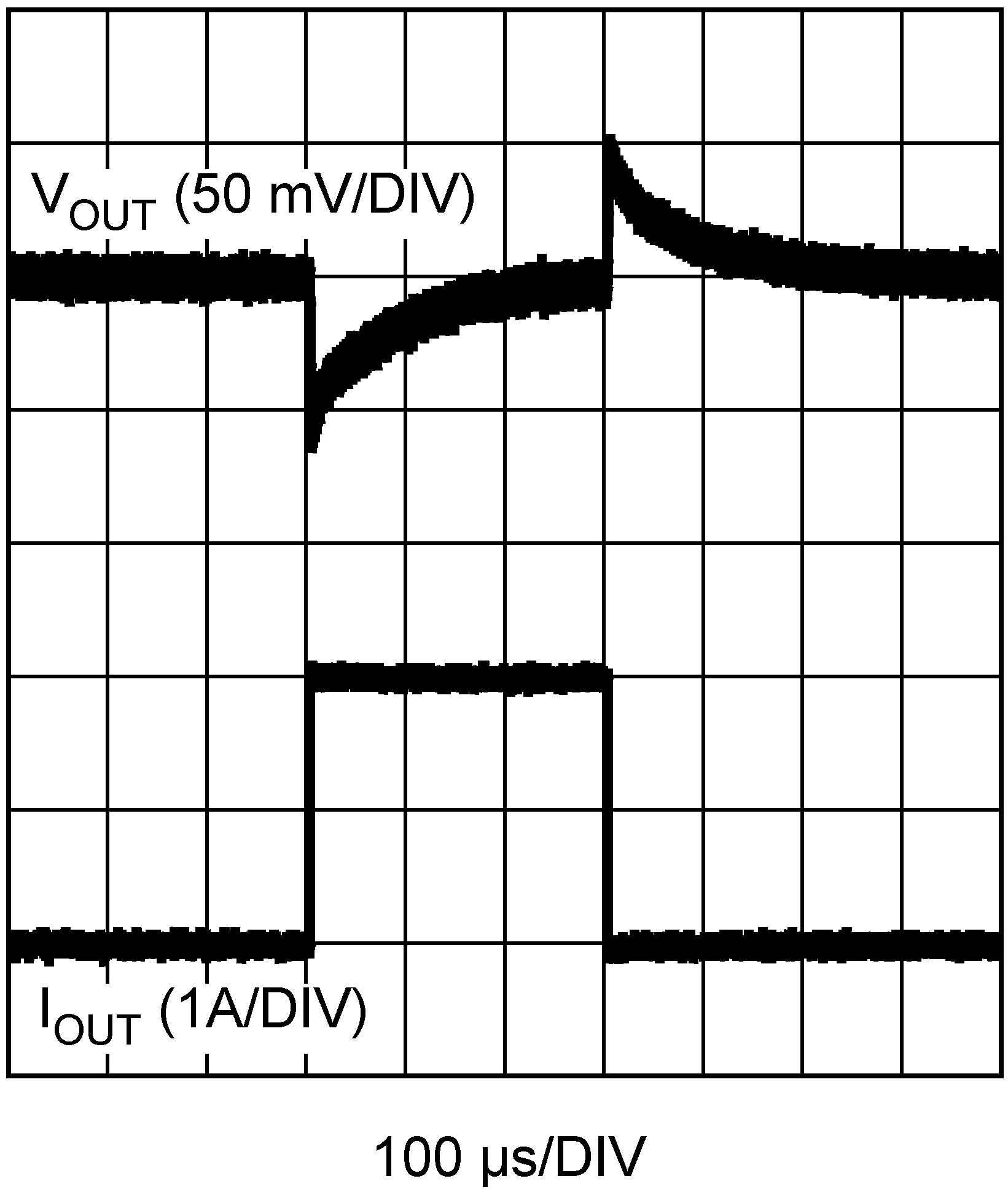
LMR12015 LMR12020 301970a5.png
VOUT = 1.8 V IOUT = 100 mA – 2 A at Slew Rate = 2 A / µs
Refer To Figure 40
Figure 34. Load Transient
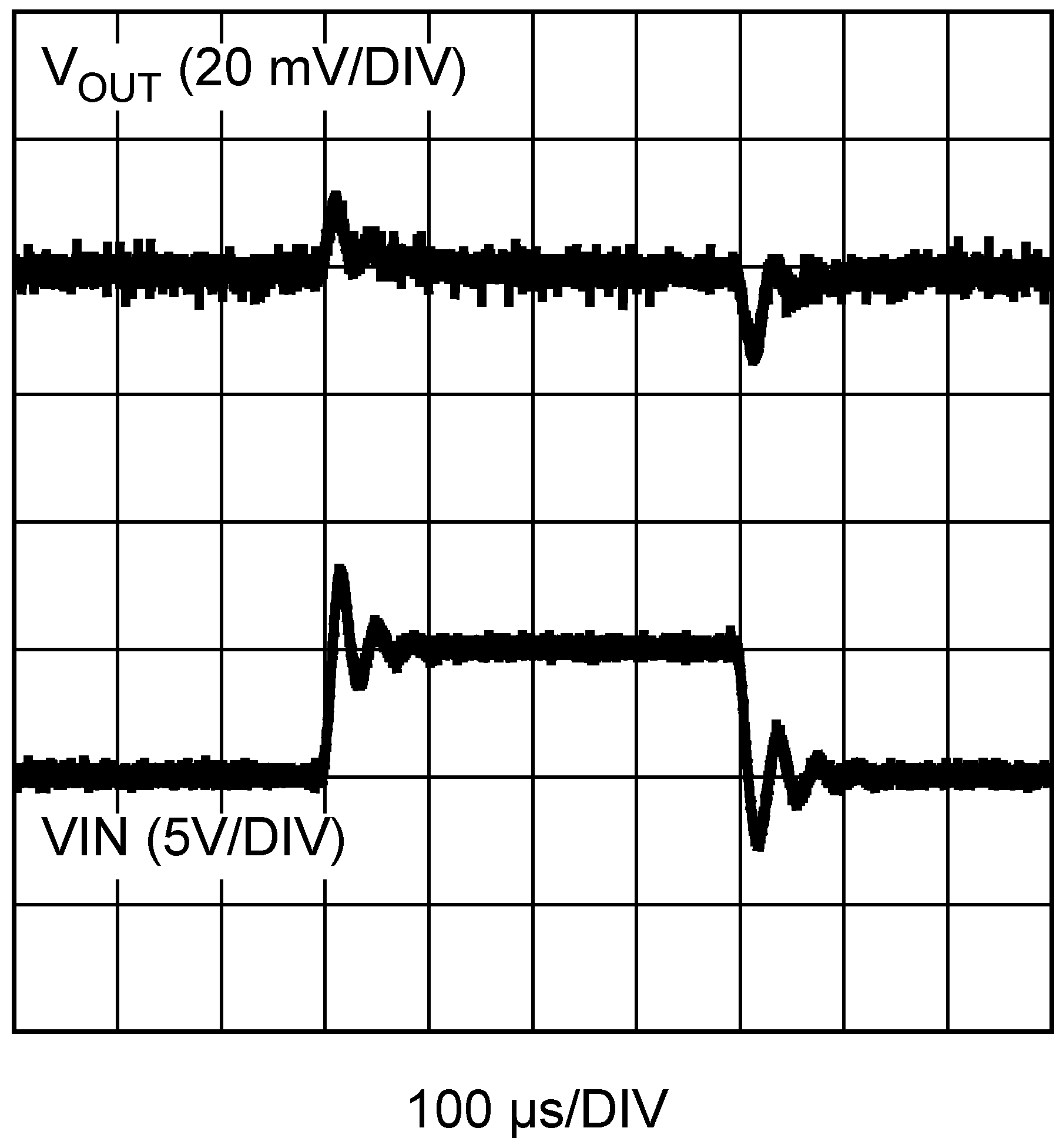
LMR12015 LMR12020 301970a8.png
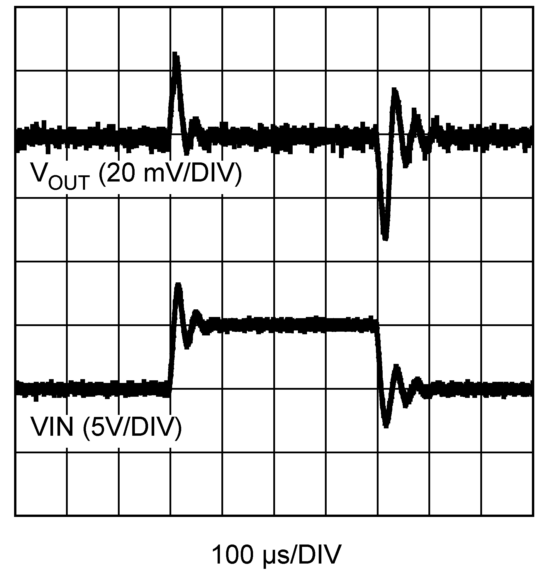
VIN = 10 to 15 V VOUT = 3.3 V No CFF
Refer To Figure 38
Figure 36. Line Transient
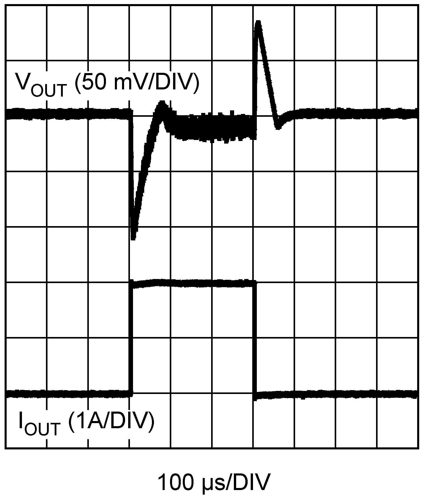
LMR12015 LMR12020 301970a3.png
VOUT = 3.3 V IOUT = 100 mA – 2 A at Slew Rate = 2 A / µs
Refer To Figure 39
Figure 33. Load Transient
LMR12015 LMR12020 301970a9.png
VIN = 10 to 15 V VOUT = 3.3 V No CFF
Refer To Figure 39
Figure 35. Line Transient