ZHCSAR9I January 2011 – December 2014 LMP91000
PRODUCTION DATA.
- 1 特性
- 2 应用
- 3 说明
- 4 修订历史记录
- 5 Pin Configuration and Functions
- 6 Specifications
-
7 Detailed Description
- 7.1 Overview
- 7.2 Functional Block Diagram
- 7.3 Feature Description
- 7.4 Device Functional Modes
- 7.5 Programming
- 7.6 Registers Maps
- 8 Application and Implementation
- 9 Power Supply Recommendations
- 10Layout
- 11器件和文档支持
- 12机械封装和可订购信息
7 Detailed Description
7.1 Overview
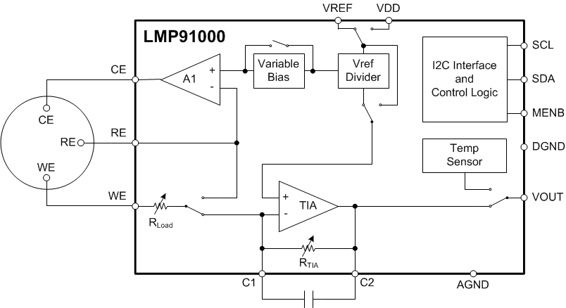
The LMP91000 is a programmable AFE for use in micropower chemical sensing applications. The LMP91000 is designed for 3-lead single gas sensors and for 2-lead galvanic cell sensors. This device provides all of the functionality for detecting changes in gas concentration based on a delta current at the working electrode. The LMP91000 generates an output voltage proportional to the cell current. Transimpedance gain is user programmable through an I2C compatible interface from 2.75 kΩ to 350 kΩ making it easy to convert current ranges from 5 µA to 750 µA full scale. Optimized for micro-power applications, the LMP91000 AFE works over a voltage range of 2.7 V to 5.25 V. The cell voltage is user selectable using the on board programmability. In addition, it is possible to connect an external transimpedance gain resistor. A temperature sensor is embedded and it can be power cycled through the interface. The output of this temperature sensor can be read by the user through the VOUT pin. It is also possible to have both temperature output and output of the TIA at the same time; the pin C2 is internally connected to the output of the transimpedance (TIA), while the temperature is available at the VOUT pin. Depending on the configuration, total current consumption for the device can be less than 10 µA. For power savings, the transimpedance amplifier can be turned off and instead a load impedance equivalent to the TIA’s inputs impedance is switched in.
7.2 Functional Block Diagram
7.3 Feature Description
7.3.1 Potentiostat Circuitry
The core of the LMP91000 is a potentiostat circuit. It consists of a differential input amplifier used to compare the potential between the working and reference electrodes to a required working bias potential (set by the Variable Bias circuitry). The error signal is amplified and applied to the counter electrode (through the Control Amplifier - A1). Any changes in the impedance between the working and reference electrodes will cause a change in the voltage applied to the counter electrode, in order to maintain the constant voltage between working and reference electrodes. A Transimpedance Amplifier connected to the working electrode, is used to provide an output voltage that is proportional to the cell current. The working electrode is held at virtual ground (Internal ground) by the transimpedance amplifier. The potentiostat will compare the reference voltage to the desired bias potential and adjust the voltage at the counter electrode to maintain the proper working-to-reference voltage.
7.3.1.1 Transimpedance Amplifier
The transimpedance amplifier (TIA) has 7 programmable internal gain resistors. This accommodates the full scale ranges of most existing sensors. Moreover an external gain resistor can be connected to the LMP91000 between C1 and C2 pins. The gain is set through the I2C interface.
7.3.1.2 Control Amplifier
The control amplifier (A1 op amp) has two tasks: a) providing initial charge to the sensor, b) providing a bias voltage to the sensor. A1 has the capability to drive up to 10 mA into the sensor in order to to provide a fast initial conditioning. A1 is able to sink and source current according to the connected gas sensor (reducing or oxidizing gas sensor). It can be powered down to reduce system power consumption. However powering down A1 is not recommended, as it may take a long time for the sensor to recover from this situation.
7.3.1.3 Variable Bias
The Variable Bias block circuitry provides the amount of bias voltage required by a biased gas sensor between its reference and working electrodes. The bias voltage can be programmed to be 1% to 24% (14 steps in total) of the supply, or of the external reference voltage. The 14 steps can be programmed through the I2C interface. The polarity of the bias can be also programmed.
7.3.1.4 Internal Zero
The internal Zero is the voltage at the non-inverting pin of the TIA. The internal zero can be programmed to be either 67%, 50% or 20%, of the supply, or the external reference voltage. This provides both sufficient headroom for the counter electrode of the sensor to swing, in case of sudden changes in the gas concentration, and best use of the ADC’s full scale input range.
The Internal zero is provided through an internal voltage divider. The divider is programmed through the I2C interface.
7.3.1.5 Temperature Sensor
The embedded temperature sensor can be switched off during gas concentration measurement to save power. The temperature measurement is triggered through the I2C interface. The temperature output is available at the VOUT pin until the configuration bit is reset. The output signal of the temperature sensor is a voltage, referred to the ground of the LMP91000 (AGND).
Table 1. Temperature Sensor Transfer
| TEMPERATURE (°C) |
OUTPUT VOLTAGE (mV) |
TEMPERATURE (°C) |
OUTPUT VOLTAGE (mV) |
|---|---|---|---|
| -40 | 1875 | 23 | 1375 |
| -39 | 1867 | 24 | 1367 |
| -38 | 1860 | 25 | 1359 |
| -37 | 1852 | 26 | 1351 |
| -36 | 1844 | 27 | 1342 |
| -35 | 1836 | 28 | 1334 |
| -34 | 1828 | 29 | 1326 |
| -33 | 1821 | 30 | 1318 |
| -32 | 1813 | 31 | 1310 |
| -31 | 1805 | 32 | 1302 |
| -30 | 1797 | 33 | 1293 |
| -29 | 1789 | 34 | 1285 |
| -28 | 1782 | 35 | 1277 |
| -27 | 1774 | 36 | 1269 |
| -26 | 1766 | 37 | 1261 |
| -25 | 1758 | 38 | 1253 |
| -24 | 1750 | 39 | 1244 |
| -23 | 1742 | 40 | 1236 |
| -22 | 1734 | 41 | 1228 |
| -21 | 1727 | 42 | 1220 |
| -20 | 1719 | 43 | 1212 |
| -19 | 1711 | 44 | 1203 |
| -18 | 1703 | 45 | 1195 |
| -17 | 1695 | 46 | 1187 |
| -16 | 1687 | 47 | 1179 |
| -15 | 1679 | 48 | 1170 |
| -14 | 1671 | 49 | 1162 |
| -13 | 1663 | 50 | 1154 |
| -12 | 1656 | 51 | 1146 |
| -11 | 1648 | 52 | 1137 |
| -10 | 1640 | 53 | 1129 |
| -9 | 1632 | 54 | 1121 |
| -8 | 1624 | 55 | 1112 |
| -7 | 1616 | 56 | 1104 |
| -6 | 1608 | 57 | 1096 |
| -5 | 1600 | 58 | 1087 |
| -4 | 1592 | 59 | 1079 |
| -3 | 1584 | 60 | 1071 |
| -2 | 1576 | 61 | 1063 |
| -1 | 1568 | 62 | 1054 |
| 0 | 1560 | 63 | 1046 |
| 1 | 1552 | 64 | 1038 |
| 2 | 1544 | 65 | 1029 |
| 3 | 1536 | 66 | 1021 |
| 4 | 1528 | 67 | 1012 |
| 5 | 1520 | 68 | 1004 |
| 6 | 1512 | 69 | 996 |
| 7 | 1504 | 70 | 987 |
| 8 | 1496 | 71 | 979 |
| 9 | 1488 | 72 | 971 |
| 10 | 1480 | 73 | 962 |
| 11 | 1472 | 74 | 954 |
| 12 | 1464 | 75 | 945 |
| 13 | 1456 | 76 | 937 |
| 14 | 1448 | 77 | 929 |
| 15 | 1440 | 78 | 920 |
| 16 | 1432 | 79 | 912 |
| 17 | 1424 | 80 | 903 |
| 18 | 1415 | 81 | 895 |
| 19 | 1407 | 82 | 886 |
| 20 | 1399 | 83 | 878 |
| 21 | 1391 | 84 | 870 |
| 22 | 1383 | 85 | 861 |
Although the temperature sensor is very linear, its response does have a slight downward parabolic shape. This shape is very accurately reflected in Table 1. For a linear approximation, a line can easily be calculated over the desired temperature range from Table 1 using the two-point equation:
where
- V is in mV, T is in °C, T1 and V1 are the coordinates of the lowest temperature
- T2 and V2 are the coordinates of the highest temperature.
For example, to determine the equation of a line over a temperature range of 20°C to 50°C, proceed as follows:
Using this method of linear approximation, the transfer function can be approximated for one or more temperature ranges of interest.
7.3.1.6 Gas Sensor Interface
The LMP91000 supports both 3-lead and 2-lead gas sensors. Most of the toxic gas sensors are amperometric cells with 3 leads (Counter, Worker and Reference). These leads should be connected to the LMP91000 in the potentiostat topology. The 2-lead gas sensor (known as galvanic cell) should be connected as simple buffer either referred to the ground of the system or referred to a reference voltage. The LMP91000 support both connections for 2-lead gas sensor.
7.3.1.6.1 3-Lead Amperometric Cell in Potentiostat Configuration
Most of the amperometric cell have 3 leads (Counter, Reference and Working electrodes). The interface of the 3-lead gas sensor to the LMP91000 is straightforward, the leads of the gas sensor need to be connected to the namesake pins of the LMP91000.
The LMP91000 is then configured in 3-lead amperometric cell mode; in this configuration the Control Amplifier (A1) is ON and provides the internal zero voltage and bias in case of biased gas sensor. The transimpedance amplifier (TIA) is ON, it converts the current generated by the gas sensor in a voltage, according to the transimpedance gain:
If different gains are required, an external resistor can be connected between the pins C1 and C2. In this case the internal feedback resistor should be programmed to “external”. The RLoad together with the output capacitance of the gas sensor acts as a low pass filter.
Figure 24. 3-Lead Amperometric Cell
7.3.1.6.2 2-Lead Galvanic Cell In Ground Referred Configuration
When the LMP91000 is interfaced to a galvanic cell (for instance to an Oxygen gas sensor) referred to the ground of the system, an external resistor needs to be placed in parallel to the gas sensor; the negative electrode of the gas sensor is connected to the ground of the system and the positive electrode to the Vref pin of the LMP91000, the working pin of the LMP91000 is connected to the ground.
The LMP91000 is then configured in 2-lead galvanic cell mode and the Vref bypass feature needs to be enabled. In this configuration the Control Amplifier (A1) is turned off, and the output of the gas sensor is amplified by the Transimpedance Amplifier (TIA) which is configured as a simple non-inverting amplifier.
The gain of this non inverting amplifier is set according the following formula:
If different gains are required, an external resistor can be connected between the pins C1 and C2. In this case the internal feedback resistor should be programmed to “external”.
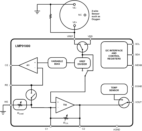 Figure 25. 2-Lead Galvanic Cell Ground-Referred
7.3.1.6.3 2-lead Galvanic Cell in Potentiostat Configuration
When the LMP91000 is interfaced to a galvanic cell (for instance to an Oxygen gas sensor) referred to a reference, the Counter and the Reference pin of the LMP91000 are shorted together and connected to negative electrode of the galvanic cell. The positive electrode of the galvanic cell is then connected to the Working pin of the LMP91000.
The LMP91000 is then configured in 3-lead amperometric cell mode (as for amperometric cell). In this configuration the Control Amplifier (A1) is ON and provides the internal zero voltage. The transimpedance amplifier (TIA) is also ON, it converts the current generated by the gas sensor in a voltage, according to the transimpedance gain:
If different gains are required, an external resistor can be connected between the pins C1 and C2. In this case the internal feedback resistor should be programmed to “external”.
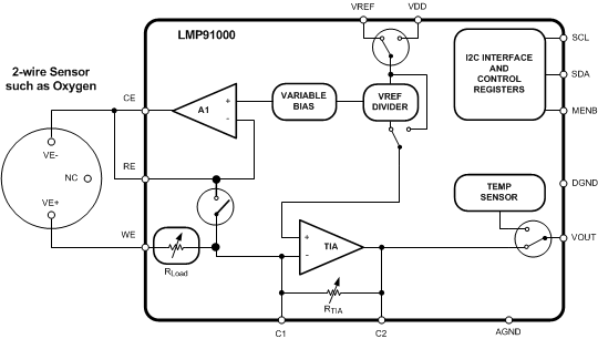 Figure 26. 2-Lead Galvanic Cell in Potentiostat Configuration
7.3.1.7 Timeout Feature
The timeout is a safety feature to avoid bus lockup situation. If SCL is stuck low for a time exceeding t_timeout, the LMP91000 will automatically reset its I2C interface. Also, in the case the LMP91000 hangs the SDA for a time exceeding t_timeout, the LMP91000’s I2C interface will be reset so that the SDA line will be released. Since the SDA is an open-drain with an external resistor pull-up, this also avoids high power consumption when LMP91000 is driving the bus and the SCL is stopped.
7.4 Device Functional Modes
The LMP91000 has 6 operational modes to optimize the current consumption and meet the needs of the applications. It is possible to select the operational mode through the I2C bus.
At the power on the LMP91000 is in deep sleep mode. In this mode the device accepts I2C commands and burns the lowest supply current. In this mode the TIA, the A1 control amplifier and the temperature sensor are OFF. This mode of operation is suggested when the gas detector is not used and a zero bias is required between WE and RE electrodes of the gas sensor. The zero bias between the WE and RE electrodes is kept by enabling the internal FET feature.
In the standby mode, the TIA is OFF, while the A1 control amplifier is ON. This mode of operation is suggested when the gas detector is not used for short amount of time and a faster warm-up of the gas detector is required.
In the 3-lead amperometric cell, the LMP91000 is configured as a standard potentiostat with A1, TIA and bias circuitry completely ON.
In the Temperature measurement (TIA OFF) the LMP91000 is in Standby mode with the Temperature sensor ON, at theVOUT pin of the LMP91000 it s possible to read the temperature sensor's output.
In the Temperature measurement (TIA ON) the LMP91000 is 3-lead amperometric cell mode with the Temperature sensor ON, at theVOUT pin of the LMP91000 it s possible to read the temperature sensor's output.
In 2-lead ground referred galvanic cell the A1 control amplifer is OFF and the Internal zero circuitry is bypassed. In this mode it is possible to connect 2-lead sensors like the O2 sensor to the LMP91000.
7.5 Programming
7.5.1 I2C Interface
The I2C compatible interface operates in Standard mode (100kHz). Pull-up resistors or current sources are required on the SCL and SDA pins to pull them high when they are not being driven low. A logic zero is transmitted by driving the output low. A logic high is transmitted by releasing the output and allowing it to be pulled-up externally. The appropriate pull-up resistor values will depend upon the total bus capacitance and operating speed. The LMP91000 comes with a 7 bit bus fixed address: 1001 000.
7.5.2 Write and Read Operation
In order to start any read or write operation with the LMP91000, MENB needs to be set low during the whole communication. Then the master generates a start condition by driving SDA from high to low while SCL is high. The start condition is always followed by a 7-bit slave address and a Read/Write bit. After these 8 bits have been transmitted by the master, SDA is released by the master and the LMP91000 either ACKs or NACKs the address. If the slave address matches, the LMP91000 ACKs the master. If the address doesn't match, the LMP91000 NACKs the master. For a write operation, the master follows the ACK by sending the 8-bit register address pointer. Then the LMP91000 ACKs the transfer by driving SDA low. Next, the master sends the 8-bit data to the LMP91000. Then the LMP91000 ACKs the transfer by driving SDA low. At this point the master should generate a stop condition and optionally set the MENB at logic high level (refer to Figure 27, Figure 28, and Figure 29).
A read operation requires the LMP91000 address pointer to be set first, also in this case the master needs setting at low logic level the MENB, then the master needs to write to the device and set the address pointer before reading from the desired register. This type of read requires a start, the slave address, a write bit, the address pointer, a Repeated Start (if appropriate), the slave address, and a read bit (refer to Figure 27, Figure 28, and Figure 29). Following this sequence, the LMP91000 sends out the 8-bit data of the register.
When just one LMP91000 is present on the I2C bus the MENB can be tied to ground (low logic level).
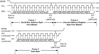 Figure 27. Register Write Transaction
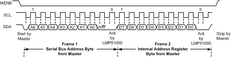 Figure 28. Pointer Set Transaction
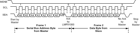 Figure 29. Register Read Transaction
7.6 Registers Maps
The registers are used to configure the LMP91000.
If writing to a reserved bit, user must write only 0. Readback value is unspecified and should be discarded.
Table 2. Register Map
| Address | Name | Power on default | Access | Lockable? |
|---|---|---|---|---|
| 0x00 | STATUS | 0x00 | Read only | No |
| 0x01 | LOCK | 0x01 | R/W | No |
| 0x02 through 0x09 | RESERVED | — | — | — |
| 0x10 | TIACN | 0x03 | R/W | Yes |
| 0x11 | REFCN | 0x20 | R/W | Yes |
| 0x12 | MODECN | 0x00 | R/W | No |
| 0x13 through 0xFF | RESERVED | — | — | — |
7.6.1 STATUS -- Status Register (Address 0x00)
The status bit is an indication of the LMP91000's power-on status. If its readback is “0”, the LMP91000 is not ready to accept other I2C commands.
| Bit | Name | Function |
|---|---|---|
| [7:1] | RESERVED | |
| 0 | STATUS | Status of Device 0 Not Ready (default) 1 Ready |
7.6.2 LOCK -- Protection Register (Address 0x01)
The lock bit enables and disables the writing of the TIACN and the REFCN registers. In order to change the content of the TIACN and the REFCN registers the lock bit needs to be set to “0”.
| Bit | Name | Function |
|---|---|---|
| [7:1] | RESERVED | |
| 0 | LOCK | Write protection 0 Registers 0x10, 0x11 in write mode 1 Registers 0x10, 0x11 in read only mode (default) |
7.6.3 TIACN -- TIA Control Register (Address 0x10)
The parameters in the TIA control register allow the configuration of the transimpedance gain (RTIA) and the load resistance (RLoad).
| Bit | Name | Function |
|---|---|---|
| [7:5] | RESERVED | RESERVED |
| [4:2] | TIA_GAIN | TIA feedback resistance selection 000 External resistance (default) 001 2.75kΩ 010 3.5kΩ 011 7kΩ 100 14kΩ 101 35kΩ 110 120kΩ 111 350kΩ |
| [1:0] | RLOAD | RLoad selection 00 10Ω 01 33Ω 10 50Ω 11 100Ω (default) |
7.6.4 REFCN -- Reference Control Register (Address 0x11)
The parameters in the Reference control register allow the configuration of the Internal zero, Bias and Reference source. When the Reference source is external, the reference is provided by a reference voltage connected to the VREF pin. In this condition the Internal Zero and the Bias voltage are defined as a percentage of VREF voltage instead of the supply voltage.
| Bit | Name | Function |
|---|---|---|
| 7 | REF_SOURCE | Reference voltage source selection 0 Internal (default) 1 external |
| [6:5] | INT_Z | Internal zero selection (Percentage of the source reference) 00 20% 01 50% (default) 10 67% 11 Internal zero circuitry bypassed (only in O2 ground referred measurement) |
| 4 | BIAS_SIGN | Selection of the Bias polarity 0 Negative (VWE – VRE)<0V (default) 1 Positive (VWE –VRE)>0V |
| [3:0] | BIAS | BIAS selection (Percentage of the source reference) 0000 0% (default) 0001 1% 0010 2% 0011 4% 0100 6% 0101 8% 0110 10% 0111 12% 1000 14% 1001 16% 1010 18% 1011 20% 1100 22% 1101 24% |
7.6.5 MODECN -- Mode Control Register (Address 0x12)
The Parameters in the Mode register allow the configuration of the Operation Mode of the LMP91000.
| Bit | Name | Function |
|---|---|---|
| 7 | FET_SHORT | Shorting FET feature 0 Disabled (default) 1 Enabled |
| [6:3] | RESERVED | |
| [2:0] | OP_MODE | Mode of Operation selection 000 Deep Sleep (default) 001 2-lead ground referred galvanic cell 010 Standby 011 3-lead amperometric cell 110 Temperature measurement (TIA OFF) 111 Temperature measurement (TIA ON) |
When the LMP91000 is in Temperature measurement (TIA ON) mode, the output of the temperature sensor is present at the VOUT pin, while the output of the potentiostat circuit is available at pin C2.