ZHCSAR9I January   2011  – December 2014 LMP91000

PRODUCTION DATA.  

  1. 特性
  2. 应用
  3. 说明
  4. 修订历史记录
  5. Pin Configuration and Functions
  6. Specifications
    1. 6.1 Absolute Maximum Ratings
    2. 6.2 ESD Ratings
    3. 6.3 Recommended Operating Conditions
    4. 6.4 Thermal Information
    5. 6.5 Electrical Characteristics
    6. 6.6 I2C Interface
    7. 6.7 Timing Requirements
    8. 6.8 Typical Characteristics
  7. Detailed Description
    1. 7.1 Overview
    2. 7.2 Functional Block Diagram
    3. 7.3 Feature Description
      1. 7.3.1 Potentiostat Circuitry
        1. 7.3.1.1 Transimpedance Amplifier
        2. 7.3.1.2 Control Amplifier
        3. 7.3.1.3 Variable Bias
        4. 7.3.1.4 Internal Zero
        5. 7.3.1.5 Temperature Sensor
        6. 7.3.1.6 Gas Sensor Interface
          1. 7.3.1.6.1 3-Lead Amperometric Cell in Potentiostat Configuration
          2. 7.3.1.6.2 2-Lead Galvanic Cell In Ground Referred Configuration
          3. 7.3.1.6.3 2-lead Galvanic Cell in Potentiostat Configuration
        7. 7.3.1.7 Timeout Feature
    4. 7.4 Device Functional Modes
    5. 7.5 Programming
      1. 7.5.1 I2C Interface
      2. 7.5.2 Write and Read Operation
    6. 7.6 Registers Maps
      1. 7.6.1 STATUS -- Status Register (Address 0x00)
      2. 7.6.2 LOCK -- Protection Register (Address 0x01)
      3. 7.6.3 TIACN -- TIA Control Register (Address 0x10)
      4. 7.6.4 REFCN -- Reference Control Register (Address 0x11)
      5. 7.6.5 MODECN -- Mode Control Register (Address 0x12)
  8. Application and Implementation
    1. 8.1 Application Information
      1. 8.1.1 Connection of More Than One LMP91000 to the I2C BUS
      2. 8.1.2 Smart Gas Sensor Analog Front-End
      3. 8.1.3 Smart Gas Sensor AFES on I2C BUS
    2. 8.2 Typical Application
      1. 8.2.1 Design Requirements
      2. 8.2.2 Detailed Design Procedure
        1. 8.2.2.1 Sensor Test Procedure
      3. 8.2.3 Application Curve
  9. Power Supply Recommendations
    1. 9.1 Power Consumption
  10. 10Layout
    1. 10.1 Layout Guidelines
    2. 10.2 Layout Example
  11. 11器件和文档支持
    1. 11.1 商标
    2. 11.2 静电放电警告
    3. 11.3 术语表
  12. 12机械封装和可订购信息

封装选项

机械数据 (封装 | 引脚)
散热焊盘机械数据 (封装 | 引脚)
订购信息

5 Pin Configuration and Functions
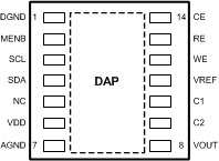
14-Pin WSON
Top View
30132502.gif

Pin Functions

PIN I/O DESCRIPTION
NAME NO.
DGND 1 G Connect to ground
MENB 2 I Module Enable, Active-Low
SCL 3 I Clock signal for I2C compatible interface
SDA 4 I/O Data for I2C compatible interface
NC 5 N/A Not Internally Connected
VDD 6 P Supply Voltage
AGND 7 G Ground
VOUT 8 O Analog Output
C2 9 N/A External filter connector (Filter between C1 and C2)
C1 10 N/A External filter connector (Filter between C1 and C2)
VREF 11 I Voltage Reference input
WE 12 I Working Electrode. Output to drive the Working Electrode of the chemical sensor
RE 13 I Reference Electrode. Input to drive Counter Electrode of the chemical sensor
CE 14 I Counter Electrode. Output to drive Counter Electrode of the chemical sensor
DAP N/C Connect to AGND