ZHCS590Q January 2011 – December 2014 LMP90097 , LMP90098 , LMP90099 , LMP90100
PRODUCTION DATA.
- 1 特性
- 2 应用
- 3 说明
- 4 典型应用电路原理图
- 5 修订历史记录
- 6 说明(续)
- 7 Pin Configuration and Functions
- 8 Specifications
-
9 Detailed Description
- 9.1 Overview
- 9.2 Functional Block Diagram
- 9.3
Feature Description
- 9.3.1 True Continuous Background Calibration
- 9.3.2 Continuous Background Sensor Diagnostics
- 9.3.3 Flexible Input MUX Channels
- 9.3.4 Programmable Gain Amplifiers (FGA and PGA)
- 9.3.5 Excitation Current Sources (IB1 and IB2) - LMP90100/LMP90098
- 9.3.6 Signal Path
- 9.3.7 Calibration
- 9.3.8 Sensor Interface
- 9.3.9 RESET and RESTART
- 9.4 Device Functional Modes
- 9.5
Programming
- 9.5.1 General Rules
- 9.5.2 Serial Digital Interface
- 9.5.3 Register Address (ADDR)
- 9.5.4 Register Read/Write Protocol
- 9.5.5 Streaming
- 9.5.6 CSB - Chip Select Bar
- 9.5.7 SPI Reset
- 9.5.8 DRDYB - Data Ready Bar
- 9.5.9 DRDYB Case1: Combining SDO/DRDYB with SDO_DRDYB_DRIVER = 0x00
- 9.5.10 DRDYB Case2: Combining SDO/DRDYB with SDO_DRDYB_DRIVER = 0x03
- 9.5.11 DRDYB Case3: Routing DRDYB to D6
- 9.5.12 Data Only Read Transaction
- 9.5.13 Cyclic Redundancy Check (CRC)
- 9.5.14 Register Read/Write Examples
- 9.5.15 Streaming Examples
- 9.6 Register Maps
- 10Application and Implementation
- 11Power Supply Recommendations
- 12Layout
- 13器件和文档支持
- 14机械封装和可订购信息
8 Specifications
8.1 Absolute Maximum Ratings
See (2)(1)(1).| MIN | MAX | UNIT | ||
|---|---|---|---|---|
| VA | Analog Supply Voltage | -0.3 | 6.0 | V |
| VIO | Digital I/O Supply Voltage | -0.3 | 6.0 | V |
| VREF | Reference Voltage | -0.3 | VA+0.3 | V |
| Voltage on Any Analog Input Pin to GND (3) | -0.3 | VA+0.3 | V | |
| Voltage on Any Digital Input PIN to GND (3) | -0.3 | VIO+0.3 | V | |
| Voltage on SDO (3) | -0.3 | VIO+0.3 | V | |
| Input Current at Any Pin (3) | 5 | mA | ||
| Output Current Source or Sink by SDO | 3 | mA | ||
| Total Package Input and Output Current | 20 | mA | ||
| TJMAX | Junction Temperature | 150 | °C | |
| Tstg | Storage Temperature | –65 | 150 | °C |
(1) For soldering specifications: see product folder at www.ti.com and SNOA549.
8.2 ESD Ratings
| VALUE | UNIT | |||
|---|---|---|---|---|
| V(ESD) | Electrostatic discharge | Human-body model (HBM), per ANSI/ESDA/JEDEC JS-001(1) | ±2500 | V |
| Charged-device model (CDM), per JEDEC specification JESD22-C101(2) | ±1250 | |||
| Machine Model (MM) | +200 | |||
(1) JEDEC document JEP155 states that 500-V HBM allows safe manufacturing with a standard ESD control process.
(2) JEDEC document JEP157 states that 250-V CDM allows safe manufacturing with a standard ESD control process.
8.3 Recommended Operating Conditions
| MIN | MAX | UNIT | ||
|---|---|---|---|---|
| VA | Analog Supply Voltage | 2.85 | 5.5 | V |
| VIO | Digital I/O Supply Voltage | 2.7 | 5.5 | V |
| VIN | Full Scale Input Range | ±VREF / PGA | V | |
| VREF | Reference Voltage | 0.5 | VA | V |
| Temperature Range for Electrical Characteristics | TMIN = –40 | TMAX = 125 | °C | |
| TA | Operating Temperature Range | –40 | 125 | °C |
8.4 Thermal Information
| THERMAL METRIC(1) | LMP90100, LMP9009x | UNIT | |
|---|---|---|---|
| PWP | |||
| 28 PINS | |||
| RθJA | Junction-to-ambient thermal resistance | 41 | °C/W |
(1) For more information about traditional and new thermal metrics, see the IC Package Thermal Metrics application report, SPRA953.
8.5 Electrical Characteristics
Unless otherwise noted, the key for the condition is (VA = VIO = VREF) / ODR (SPS) / buffer / calibration / gain. The typical values apply for TA = 25°C.| PARAMETER | TEST CONDITIONS | MIN | TYP | MAX | UNIT | ||
|---|---|---|---|---|---|---|---|
| n | Resolution | 24 | Bits | ||||
| ENOB / NFR | Effective Number of Bits and Noise Free Resolution | 3V / all / ON / OFF / all. Shorted input. | Table 1 | Bits | |||
| 5V / all / ON / OFF / all. Shorted input. | Table 2 | Bits | |||||
| ODR | Output Data Rates | 1.6675 | Table 1 | 214.6 | SPS | ||
| Gain | FGA × PGA | 1 | Table 1 | 128 | |||
| INL | Integral Non-Linearity(1) | 3V / 214.65 / ON / ON / 1 | -15 | ± 7 | +15 | ppm | |
| 3V & 5V / 214.65 / ON / ON / 16 | ± 15 | ppm | |||||
| Total Noise | 3V / all / ON / ON / all. Shorted input. | Table 1 | µV | ||||
| 5V / all / ON / OFF / all. Shorted input. | Table 3 | µV | |||||
| OE | Offset Error | 3V & 5V / all / ON or OFF / ON / all | Below Noise Floor (rms) | µV | |||
| 3V / 214.65 / ON / ON / 1 | 1.22 | 9.52 | µV | ||||
| 3V / 214.65 / ON / ON / 128 | 0.00838 | 0.70 | µV | ||||
| 5V / 214.65 / ON / ON / 1 | 1.79 | 8.25 | µV | ||||
| 5V / 214.65 / ON / ON / 128 | 0.0112 | 0.63 | µV | ||||
| Offset Drift Over Temp(1) | 3V & 5V / 214.65 / ON or OFF / OFF / 1-8 | 100 | nV/°C | ||||
| 3V & 5V / 214.65 / ON / ON / 1-8 | 3 | nV/°C | |||||
| 3V & 5V / 214.65 / ON / OFF / 16 | 25 | nV/°C | |||||
| 3V & 5V / 214.65 / ON / ON / 16 | 0.4 | nV/°C | |||||
| 3V & 5V / 214.65 / ON / OFF / 128 | 6 | nV/°C | |||||
| 3V & 5V / 214.65 / ON / ON / 128 | 0.125 | nV/°C | |||||
| Offset Drift over Time (1) | 5V / 214.65 / ON / OFF / 1, TA = 150°C | 2360 | nV / 1000 hours | ||||
| 5V / 214.65 / ON / ON / 1, TA = 150°C | 100 | nV / 1000 hours | |||||
| GE | Gain Error(1) | 3V & 5V / 214.65 / ON / ON / 1 | 25°C | 7 | ppm | ||
| Full Range | -80 | 80 | |||||
| 3V & 5V / 13.42 / ON / ON / 16 | 50 | ppm | |||||
| 3V & 5V / 13.42 / ON / ON / 64 | 50 | ppm | |||||
| 3V & 5V / 13.42 / ON / ON / 128 | 100 | ppm | |||||
| Gain Drift over Temp (1) | 3V & 5V / 214.65 / ON / ON / all | 0.5 | ppm/°C | ||||
| Gain Drift over Time (1) | 5V / 214.65 / ON / OFF / 1, TA = 150°C | 5.9 | ppm / 1000 hours | ||||
| 5V / 214.65 / ON / ON / 1, TA = 150°C | 1.6 | ppm / 1000 hours | |||||
| CONVERTER'S CHARACTERISTIC | |||||||
| CMRR | Input Common Mode Rejection Ratio | DC, 3V / 214.65 / ON / ON / 1 | 25°C | 117 | dB | ||
| Full Range | 70 | ||||||
| DC, 5V / 214.65 / OFF / OFF / 1 | 25°C | 120 | dB | ||||
| Full Range | 90 | ||||||
| 50/60 Hz, 5V / 214.65 / OFF / OFF / 1 | 117 | dB | |||||
| Reference Common Mode Rejection | VREF = 2.5V | 101 | dB | ||||
| PSRR | Power Supply Rejection Ratio | DC, 3V / 214.65 / ON / ON / 1 | 75 | 115 | dB | ||
| DC, 5V / 214.65 / ON / ON / 1 | 112 | dB | |||||
| NMRR | Normal Mode Rejection Ratio (1) | 47 Hz to 63 Hz, 5V / 13.42 / OFF / OFF / 1 | 25°C | dB | |||
| Full Range | 78 | ||||||
| Cross-talk(1) | 3V / 214.65 / OFF / OFF / 1 | 25°C | 136 | dB | |||
| Full Range | 95 | ||||||
| 5V / 214.65 / OFF / OFF / 1 | 25°C | 143 | dB | ||||
| Full Range | 95 | ||||||
| POWER SUPPLY CHARACTERISTICS | |||||||
| VA | Analog Supply Voltage | 2.85 | 3.0 | 5.5 | V | ||
| VIO | Digital Supply Voltage | 2.7 | 3.3 | 5.5 | V | ||
| IVA | Analog Supply Current | 3V / 13.42 / OFF / OFF / 1, ext. CLK | 25°C | 400 | µA | ||
| Full Range | 500 | ||||||
| 5V / 13.42 / OFF / OFF / 1, ext. CLK | 25°C | 464 | µA | ||||
| Full Range | 555 | ||||||
| 3V / 13.42 / ON / OFF / 64, ext. CLK | 25°C | 600 | µA | ||||
| Full Range | 700 | ||||||
| 5V / 13.42 / ON / OFF / 64, ext. CLK | 25°C | 690 | µA | ||||
| Full Range | 800 | ||||||
| 3V / 214.65 / ON / OFF / 64, int. CLK | 25°C | 1547 | µA | ||||
| Full Range | 1700 | ||||||
| 5V / 214.65 / ON / OFF / 64, int. CLK | 25°C | 1760 | µA | ||||
| Full Range | 2000 | ||||||
| 3V / 214.65 / OFF / OFF / 1, int. CLK | 25°C | 826 | µA | ||||
| Full Range | 1000 | ||||||
| 5V / 214.65 / OFF / OFF / 1, int. CLK | 25°C | 941 | µA | ||||
| Full Range | 1100 | ||||||
| Standby, 3V , int. CLK | 3 | 10 | µA | ||||
| Standby, 3V , ext. CLK | 257 | µA | |||||
| Standby, 5V, int. CLK | 5 | 15 | µA | ||||
| Standby, 3V, ext. CLK | 300 | µA | |||||
| Power-down, 3 V, int/ext CLK | 25°C | 2.6 | µA | ||||
| Full Range | 5 | ||||||
| Power-down, 5 V, int/ext CLK | 25°C | 4.6 | µA | ||||
| Full Range | 9 | ||||||
| REFERENCE INPUT | |||||||
| VREFP | Positive Reference | VREFN + 0.5 | VA | V | |||
| VREFN | Negative Reference | GND | VREFP - 0.5 | V | |||
| VREF | Differential Reference | VREF = VREFP - VREFN | 0.5 | VA | V | ||
| ZREF | Reference Impedance | 3 V / 13.42 / OFF / OFF / 1 | 10 | MΩ | |||
| IREF | Reference Input | 3 V / 13.42 / ON or OFF / ON or OFF / all | ±2 | µA | |||
| CREFP | Capacitance of the Positive Reference | See (1), gain = 1 | 6 | pF | |||
| CREFN | Capacitance of the Negative Reference | See (1), gain = 1 | 6 | pF | |||
| ILREF | Reference Leakage Current | Power-down | 1 | nA | |||
| ANALOG INPUT | |||||||
| VINP | Positive Input | Gain = 1-8, buffer ON | GND + 0.1 | VA - 0.1 | V | ||
| Gain = 16 - 128, buffer ON | GND + 0.4 | VA - 1.5 | V | ||||
| Gain = 1-8, buffer OFF | GND | VA | V | ||||
| VINN | Negative Input | Gain = 1-8, buffer ON | GND + 0.1 | VA - 0.1 | V | ||
| Gain = 16 - 128, buffer ON | GND + 0.4 | VA - 1.5 | V | ||||
| Gain = 1-8, buffer OFF | GND | VA | V | ||||
| VIN | Differential Input | VIN = VINP - VINN | ±VREF / PGA | ||||
| ZIN | Differential Input Impedance | ODR = 13.42 SPS | 15.4 | MΩ | |||
| CINP | Capacitance of the Positive Input | 5V / 214.65 / OFF / OFF / 1 | 4 | pF | |||
| CINN | Capacitance of the Negative Input | 5V / 214.65 / OFF / OFF / 1 | 4 | pF | |||
| IIN | Input Leakage Current | 3V & 5V / 13.42 / ON / OFF / 1-8 | 500 | pA | |||
| 3V & 5V / 13.42 / ON / OFF / 16 - 128 | 100 | pA | |||||
| DIGITAL INPUT CHARACTERISTICS at VA = VIO = VREF = 3.0V | |||||||
| VIH | Logical "1" Input Voltage | 0.7 x VIO | V | ||||
| VIL | Logical "0" Input Voltage | 0.3 x VIO | V | ||||
| IIL | Digital Input Leakage Current | -10 | +10 | µA | |||
| VHYST | Digital Input Hysteresis | 0.1 x VIO | V | ||||
| DIGITAL OUTPUT CHARACTERISTICS at VA = VIO = VREF = 3.0V | |||||||
| VOH | Logical "1" Output Voltage | Source 300 µA | 2.6 | V | |||
| VOL | Logical "0" Output Voltage | Sink 300 µA | 0.4 | V | |||
| IOZH, IOZL | Tri-state Leakage Current | -10 | 10 | µA | |||
| COUT | Tri-state Capacitance | See (1) | 5 | pF | |||
| EXCITATION CURRENT SOURCES CHARACTERISTICS (LMP90100/LMP90098 only) | |||||||
| IB1, IB2 | Excitation Current Source Output | 0, 100, 200, 300, 400, 500, 600, 700, 800, 900, 1000 | µA | ||||
| IB1/IB2 Tolerance | VA = VREF = 3 V | 25°C | 2.5% | ||||
| Full Range | -7% | 7% | |||||
| VA = VREF = 5 V | 25°C | 0.2% | |||||
| Full Range | -3.5% | 3.5% | |||||
| IB1/IB2 Output Compliance Range | VA = 3.0 V & 5.0 V, IB1/IB2 = 100 µA to 1000 µA | VA - 0.8 | V | ||||
| IB1/IB2 Regulation | VA = 5.0 V, IB1/IB2 = 100 µA to 1000 µA | 0.07 | % / V | ||||
| IBTC | IB1/IB2 Drift | VA = 3.0 V | 95 | ppm/°C | |||
| VA = 5.0 V | 60 | ppm/°C | |||||
| IBMT | IB1/IB2 Matching | 3 V and 5 V / 214.65 / OFF / OFF / 1, IB1/IB2 = 100 µA | 25°C | 0.34% | |||
| Full Range | 1.53% | ||||||
| 3 V and 5 V / 214.65 / OFF / OFF / 1, IB1/IB2 = 200 µA | 25°C | 0.22% | |||||
| Full Range | 1% | ||||||
| 3V & 5V / 214.65 / OFF / OFF / 1, IB1/IB2 = 300 µA | 25°C | 0.2% | |||||
| Full Range | 0.85% | ||||||
| 3 V and 5 V / 214.65 / OFF / OFF / 1, IB1/IB2 = 400 µA | 25°C | 0.15% | |||||
| Full Range | 0.8% | ||||||
| 3 V and 5 V / 214.65 / OFF / OFF / 1, IB1/IB2 = 500 µA | 25°C | 0.14% | |||||
| Full Range | 0.7% | ||||||
| 3 V and 5 V / 214.65 / OFF / OFF / 1, IB1/IB2 = 600 µA | 25°C | 0.13% | |||||
| Full Range | 0.7% | ||||||
| 3 V and 5 V / 214.65 / OFF / OFF / 1, IB1/IB2 = 700 µA | 25°C | 0.075% | |||||
| Full Range | 0.65% | ||||||
| 3 V and 5 V / 214.65 / OFF / OFF / 1, IB1/IB2 = 800 µA | 25°C | 0.085% | |||||
| Full Range | 0.6% | ||||||
| 3 V and 5 V / 214.65 / OFF / OFF / 1, IB1/IB2 = 900 µA | 0.11% | 0.55%(2) | |||||
| 3 V and 5 V / 214.65 / OFF / OFF / 1, IB1/IB2 = 1000 µA | 0.11% | 0.45%(2) | |||||
| IBMTC | IB1/IB2 Matching Drift | VA = 3.0 V and 5.0 V, IB1/IB2 = 100 µA to 1000 µA | 2 | ppm/°C | |||
| INTERNAL/EXTERNAL CLK | |||||||
| CLKIN | Internal Clock Frequency | 893 | kHz | ||||
| CLKEXT | External Clock Frequency | See (1) | 1.8 | 3.5717 | 7.2 | MHz | |
| External Crystal Frequency | Input Low Voltage | 0 | V | ||||
| Input High Voltage | 1 | V | |||||
| Frequency | 1.8 | 3.5717 | 7.2 | MHz | |||
| Start-up time | 7 | ms | |||||
| SCLK | Serial Clock | 10 | MHz | ||||
(1) This parameter is specified by design and/or characterization and is not tested in production
(2) Limits apply for TMIN ≤ TA ≤ TMAX
Table 1. ENOB (Noise Free Resolution) vs. Sampling Rate and Gain at VA = VIO = VREF = 3 V
| ODR (SPS) | Gain of the ADC | |||||||
|---|---|---|---|---|---|---|---|---|
| 1 | 2 | 4 | 8 | 16 | 32 | 64 | 128 | |
| 1.6775 | 20.5 (18) | 20.5 (18) | 19.5 (17) | 19 (16.5) | 20.5 (18) | 19.5 (17) | 19 (16.5) | 18 (15.5) |
| 3.355 | 20 (17.5) | 20 (17.5) | 19 (16.5) | 18.5 (16) | 20 (17.5) | 19 (16.5) | 18.5 (16) | 17 (14.5) |
| 6.71 | 19.5 (17) | 19.5 (17) | 18.5 (16) | 18 (15.5) | 19.5 (17) | 18.5 (16) | 17.5 (15) | 17 (14.5) |
| 13.42 | 19 (16.5) | 18.5 (16) | 18 (15.5) | 17.5 (15) | 19 (16.5) | 18 (15.5) | 17.5 (15) | 16.5 (14) |
| 26.83125 | 20.5 (18) | 20 (17.5) | 19.5 (17) | 19 (16.5) | 20 (17.5) | 19 (16.5) | 18 (15.5) | 17.5 (15) |
| 53.6625 | 20 (17.5) | 19.5 (17) | 19 (16.5) | 18.5 (16) | 19.5 (17) | 18.5 (16) | 17.5 (15) | 17 (14.5) |
| 107.325 | 19.5 (17) | 19 (16.5) | 18.5 (16) | 18 (15.5) | 19 (16.5) | 18 (15.5) | 17 (14.5) | 16.5 (14) |
| 214.65 | 19 (16.5) | 18.5 (16) | 18 (15.5) | 17.5 (15) | 18.5 (16) | 17.5 (15) | 17 (14.5) | 16 (13.5) |
Table 2. RMS Noise (µV) vs. Sampling Rate and Gain at VA = VIO = VREF = 3 V
| ODR (SPS) | Gain of the ADC | |||||||
|---|---|---|---|---|---|---|---|---|
| 1 | 2 | 4 | 8 | 16 | 32 | 64 | 128 | |
| 1.6775 | 3.08 | 1.90 | 1.53 | 1.27 | 0.23 | 0.21 | 0.15 | 0.14 |
| 3.355 | 4.56 | 2.70 | 2.21 | 1.67 | 0.34 | 0.27 | 0.24 | 0.26 |
| 6.71 | 6.15 | 4.10 | 3.16 | 2.39 | 0.51 | 0.40 | 0.37 | 0.35 |
| 13.42 | 8.60 | 5.85 | 4.29 | 3.64 | 0.67 | 0.54 | 0.51 | 0.49 |
| 26.83125 | 3.35 | 2.24 | 1.65 | 1.33 | 0.33 | 0.27 | 0.26 | 0.25 |
| 53.6625 | 4.81 | 3.11 | 2.37 | 1.90 | 0.44 | 0.39 | 0.37 | 0.36 |
| 107.325 | 6.74 | 4.51 | 3.38 | 2.66 | 0.63 | 0.54 | 0.52 | 0.49 |
| 214.65 | 9.52 | 6.37 | 4.72 | 3.79 | 0.90 | 0.79 | 0.72 | 0.70 |
Table 3. ENOB (Noise Free Resolution) vs. Sampling Rate and Gain at VA = VIO = VREF = 5 V
| SPS | Gain of the ADC | |||||||
|---|---|---|---|---|---|---|---|---|
| 1 | 2 | 4 | 8 | 16 | 32 | 64 | 128 | |
| 1.6775 | 21.5 (19) | 21.5 (19) | 20.5 (18) | 20 (17.5) | 21 (18.5) | 20.5 (18) | 19.5 (17) | 18.5 (16) |
| 3.355 | 21 (18.5) | 21 (18.5) | 20 (17.5) | 19.5 (17) | 20.5 (18) | 20 (17.5) | 19 (16.5) | 18 (15.5) |
| 6.71 | 20.5 (18) | 20 (17.5) | 19.5 (17) | 19 (16.5) | 20 (17.5) | 19.5 (17) | 19 (16.5) | 17.5 (15) |
| 13.42 | 20 (17.5) | 19.5 (17) | 19 (16.5) | 18.5 (16) | 20 (17.5) | 19 (16.5) | 18 (15.5) | 17.5 (15) |
| 26.83125 | 21.5 (19) | 21 (18.5) | 20.5 (18) | 20 (17.5) | 21 (18.5) | 20 (17.5) | 19.5 (17) | 18 (15.5) |
| 53.6625 | 21 (18.5) | 20.5 (18) | 20 (17.5) | 19.5 (17) | 20.5 (18) | 19.5 (17) | 18.5 (16) | 17.5 (15) |
| 107.325 | 20.5 (18) | 20 (17.5) | 19.5 (17) | 19 (16.5) | 20 (17.5) | 19 (16.5) | 18 (15.5) | 17 (14.5) |
| 214.65 | 20 (17.5) | 19.5 (17) | 19 (16.5) | 18.5 (16) | 19.5 (17) | 18.5 (16) | 17.5 (15) | 16.5 (14) |
Table 4. RMS Noise (µV) vs. Sampling Rate and Gain at VA = VIO = VREF = 5 V
| SPS | Gain of the ADC | |||||||
|---|---|---|---|---|---|---|---|---|
| 1 | 2 | 4 | 8 | 16 | 32 | 64 | 128 | |
| 1.6775 | 2.68 | 1.65 | 1.24 | 1.00 | 0.22 | 0.19 | 0.17 | 0.16 |
| 3.355 | 3.86 | 2.36 | 1.78 | 1.47 | 0.34 | 0.27 | 0.22 | 0.22 |
| 6.71 | 5.23 | 3.49 | 2.47 | 2.09 | 0.44 | 0.34 | 0.30 | 0.32 |
| 13.42 | 7.94 | 5.01 | 3.74 | 2.94 | 0.61 | 0.50 | 0.45 | 0.43 |
| 26.83125 | 2.90 | 1.86 | 1.34 | 1.08 | 0.29 | 0.24 | 0.23 | 0.23 |
| 53.6625 | 4.11 | 2.60 | 1.90 | 1.50 | 0.39 | 0.35 | 0.32 | 0.31 |
| 107.325 | 5.74 | 3.72 | 2.72 | 2.11 | 0.56 | 0.48 | 0.46 | 0.44 |
| 214.65 | 8.25 | 5.31 | 3.82 | 2.97 | 0.79 | 0.68 | 0.64 | 0.63 |
8.6 SPI Timing Requirements
Unless otherwise noted, specified limits apply for VA = VIO = 3.0 V.| MIN | NOM | MAX | UNIT | ||
|---|---|---|---|---|---|
| fSCLK | 10 | MHz | |||
| tCH | SCLK High time | 0.4 / fSCLK | ns | ||
| tCL | SCLK Low time | 0.4 / fSCLK | ns |
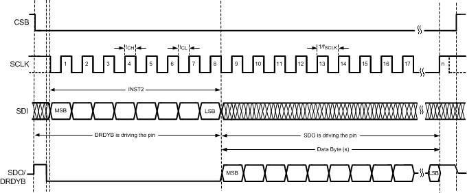 Figure 1. SPI Timing Diagram
8.7 CBS Setup and Hold Timing Requirements
Unless otherwise noted, specified limits apply for VA = VIO = 3.0 V.| MIN | NOM | MAX | UNIT | ||
|---|---|---|---|---|---|
| tCSSU | CSB Setup time prior to an SCLK rising edge | 5 | ns | ||
| tCSH | CSB Hold time after the last rising edge of SCLK | 6 | ns |
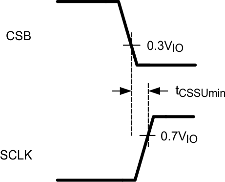 Figure 2. CBS Setup Time
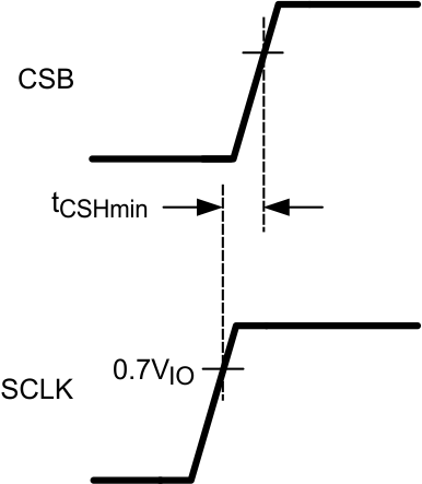 Figure 3. CSB Hold Time
8.8 SDI Timing Requirements
Unless otherwise noted, specified limits apply for VA = VIO = 3.0 V.| MIN | NOM | MAX | UNIT | ||
|---|---|---|---|---|---|
| tCLKR | SCLK Rise time | 1.15 | ns | ||
| tCLKF | SCLK Fall time | 1.15 | ns | ||
| tDISU | SDI Setup time prior to an SCLK rising edge | 5 | ns | ||
| tDIH | SDI Hold time after an SCLK rising edge | 6 | ns |
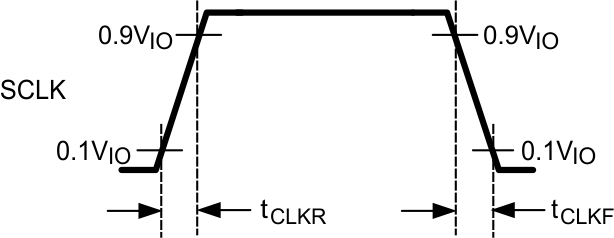 Figure 4. SCLK Rise and Fall Time
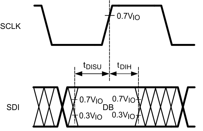 Figure 5. SDI Setup and Hold Time
8.9 SDO Timing Requirements
Unless otherwise noted, specified limits apply for VA = VIO = 3.0 V.| MIN | NOM | MAX | UNIT | |||
|---|---|---|---|---|---|---|
| tDOE | SDO Enable time from the falling edge of the 8th SCLK | 35 | ns | |||
| tDOR | SDO Rise time | See (1) | 7 | ns | ||
| tDOF | SDO Fall time | See (1) | 7 | ns | ||
| tDRDYB | Data Ready Bar pulse at every 1/ODR second, see Figure 58 |
ODR ≤ 13.42 SPS | 64 | µs | ||
| 13.42 < ODR ≤ 214.65 SPS | 4 | µs | ||||
(1) Absolute Maximum Ratings indicate limits beyond which damage to the device may occur. Recommended Operating Conditions indicate conditions for which the device is functional, but do not ensure specific performance limits. For ensured specifications and test conditions, see the Electrical Characteristics. The ensured specifications apply only for the test conditions listed. Some performance characteristics may degrade when the device is not operated under the listed test conditions.
(2) All voltages are measured with respect to GND, unless otherwise specified
(3) When the input voltage (VIN) exceeds the power supply (VIN < GND or VIN > VA), the current at that pin must be limited to 5mA and VIN has to be within the Absolute Maximum Rating for that pin. The 20 mA package input current rating limits the number of pins that can safely exceed the power supplies with current flow to four pins.
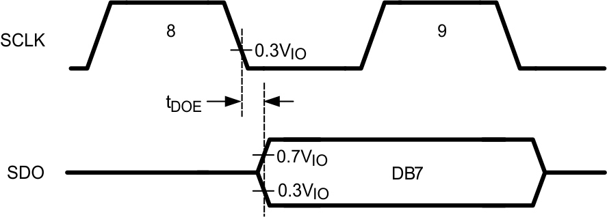 Figure 6. SDO Enable Time
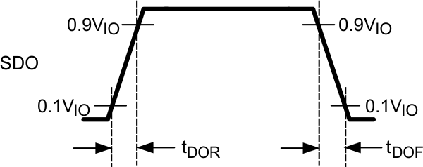 Figure 7. SDO Rise and Fall Time
8.10 Typical Characteristics
Unless otherwise noted, specified limits apply for VA = VIO = VREF = 3.0 V. The maximum and minimum values apply for TA = TMIN to TMAX; the typical values apply for TA = 25°C.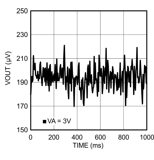 Figure 8. Noise Measurement Without Calibration
at Gain = 1
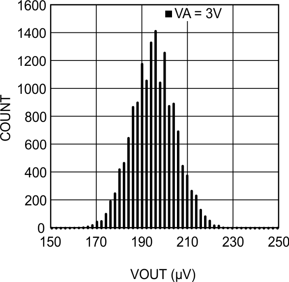 Figure 10. Histogram Without Calibration at Gain = 1
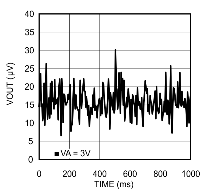 Figure 12. Noise Measurement Without Calibration
at Gain = 8
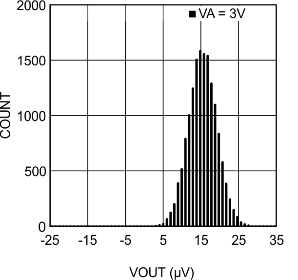 Figure 14. Histogram Without Calibration at Gain = 8
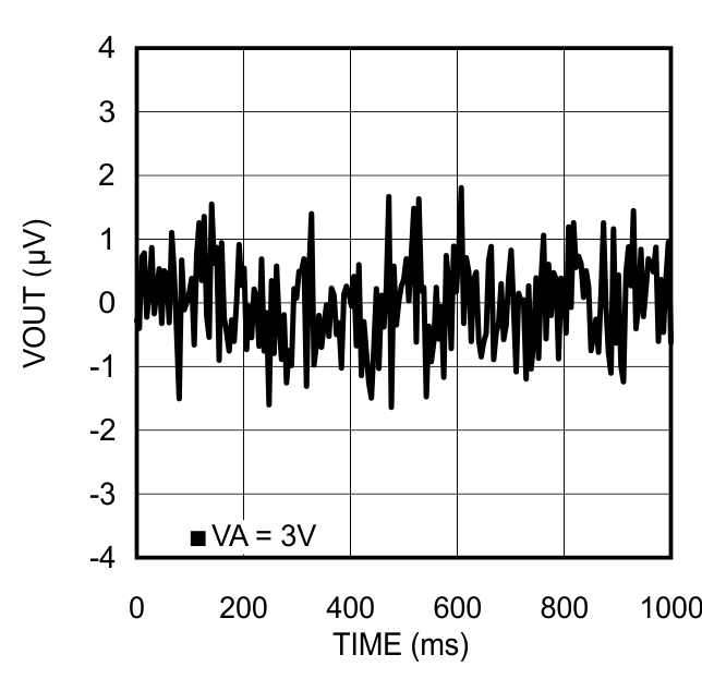 Figure 16. Noise Measurement Without Calibration
 at Gain = 128
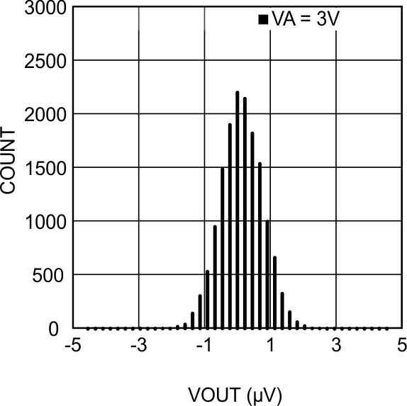 Figure 18. Histogram Without Calibration at Gain = 128
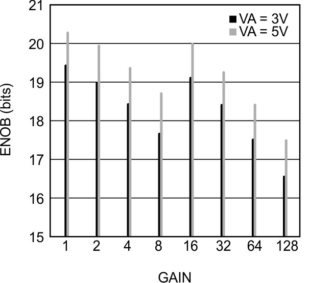 Figure 20. ENOB vs. Gain Without Calibration
 at ODR = 13.42 SPS
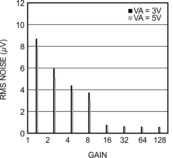 Figure 22. Noise vs. Gain Without Calibration
 at ODR = 13.42 SPS
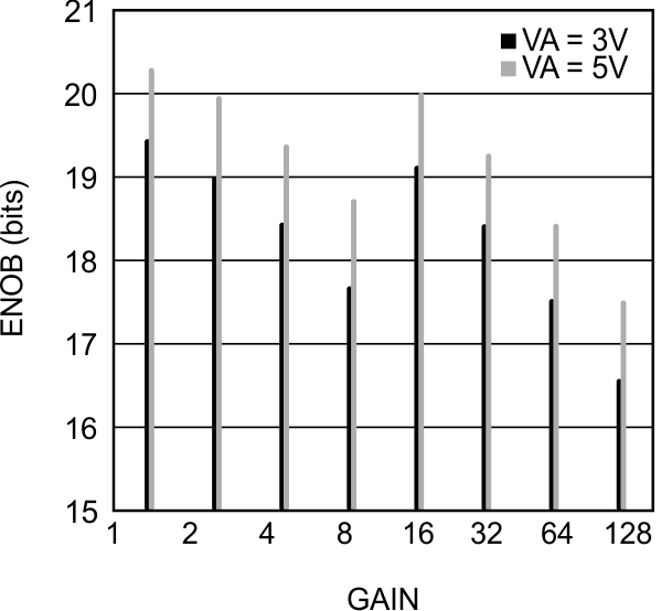 Figure 24. ENOB vs. Gain Without Calibration
 at ODR = 214.65 SPS
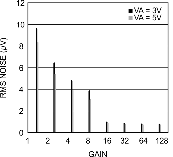 Figure 26. Noise vs. Gain Without Calibration
 at ODR = 214.65 SPS
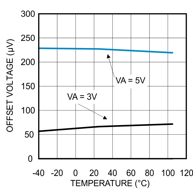 Figure 28. Offset Error vs. Temperature Without Calibration at Gain = 1
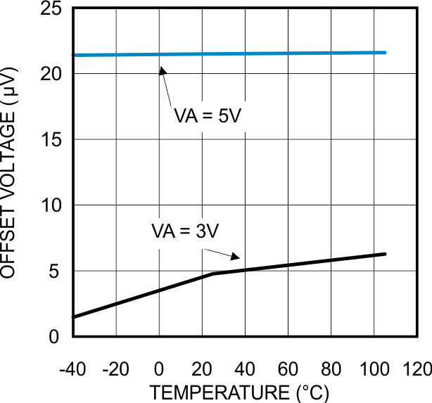 Figure 30. Offset Error vs. Temperature Without Calibration at Gain = 8
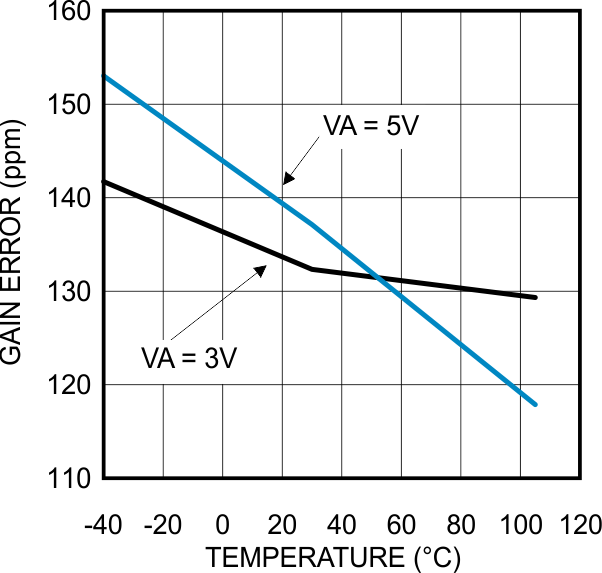 Figure 32. Gain Error vs. Temperature Without Calibration
 at Gain = 1
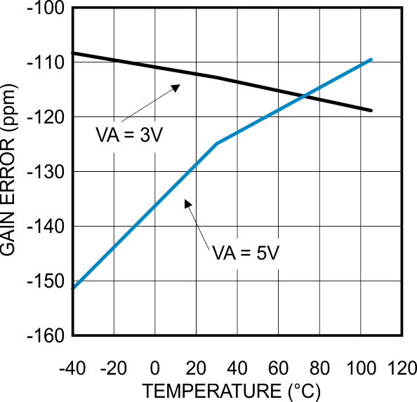 Figure 34. Gain Error vs. Temperature Without Calibration
 at Gain = 8
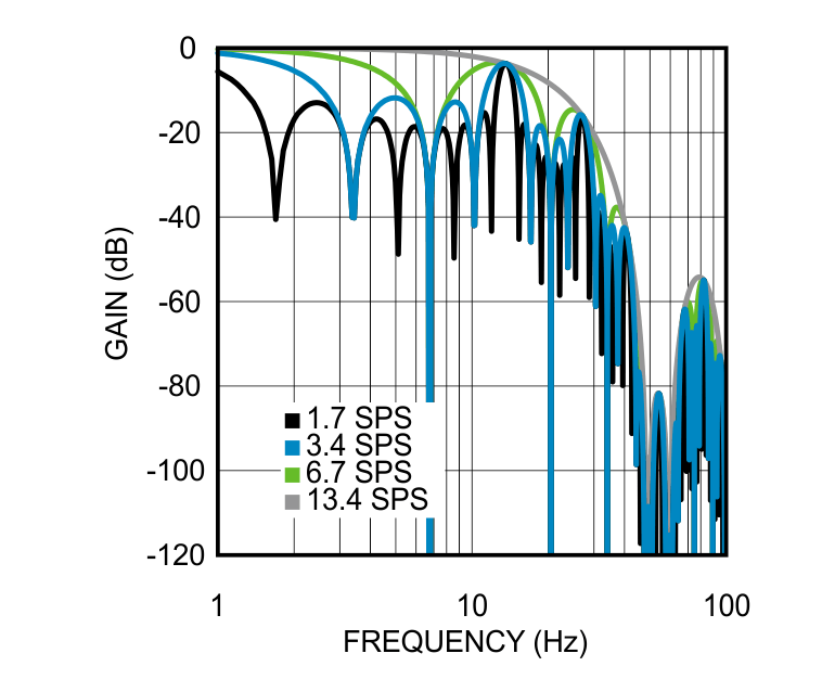 Figure 36. Digital Filter Frequency Response
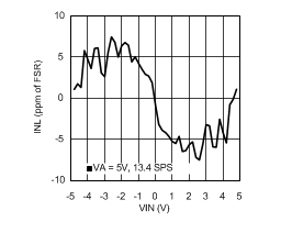 Figure 38. INL at Gain = 1
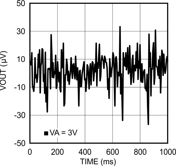 Figure 9. Noise Measurement With Calibration
at Gain = 1
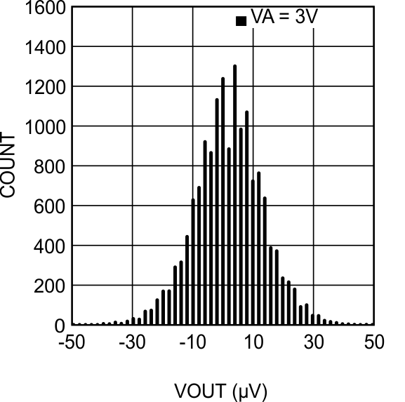 Figure 11. Histogram With Calibration at Gain = 1
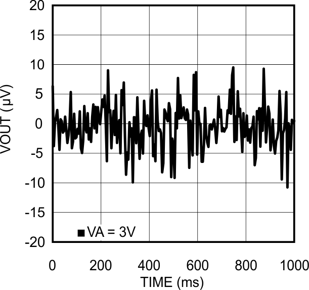 Figure 13. Noise Measurement With Calibration
at Gain = 8
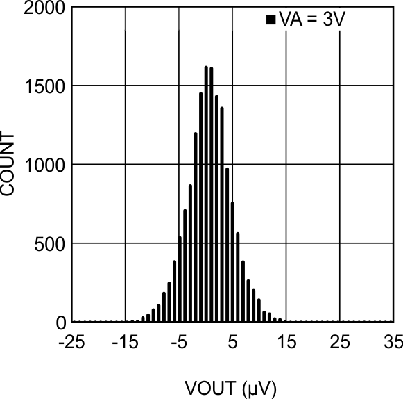 Figure 15. Histogram With Calibration at Gain = 8
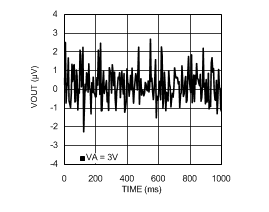 Figure 17. Noise Measurement With Calibration
 at Gain = 128
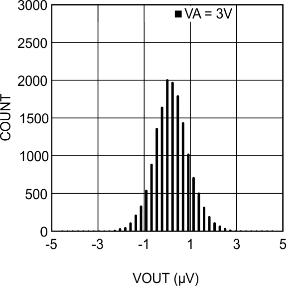 Figure 19. Histogram With Calibration at Gain = 128
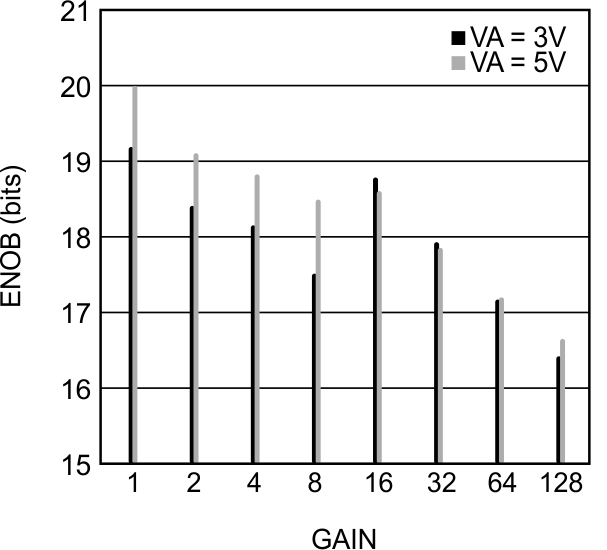 Figure 21. ENOB vs. Gain With Calibration
 at ODR = 13.42 SPS
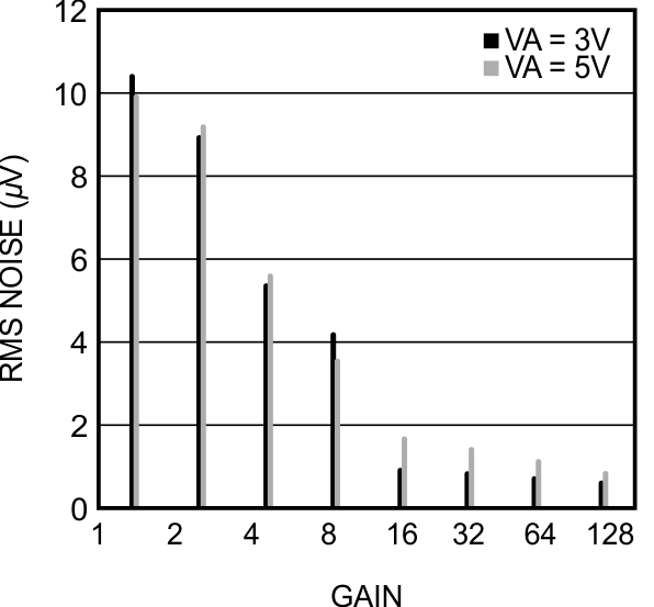 Figure 23. Noise vs. Gain With Calibration
 at ODR = 13.42 SPS
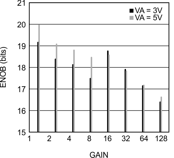 Figure 25. ENOB vs. Gain With Calibration
 at ODR = 214.65 SPS
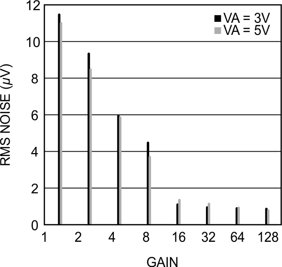 Figure 27. Noise vs. Gain With Calibration
 at ODR = 214.65 SPS
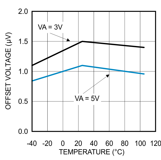 Figure 29. Offset Error vs. Temperature With Calibration at Gain = 1
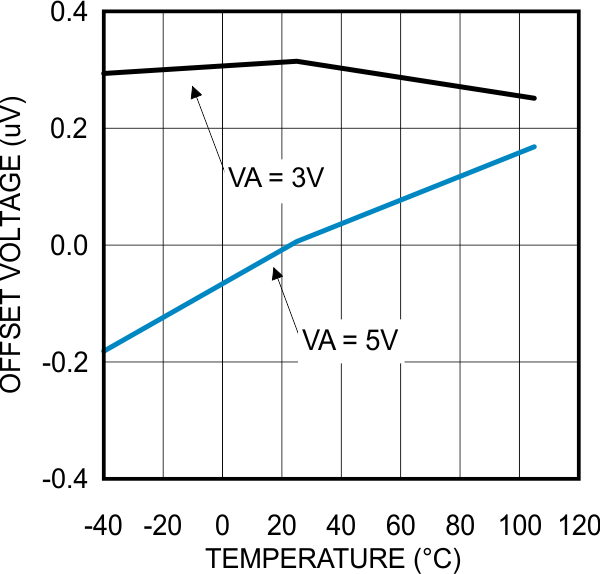 Figure 31. Offset Error vs. Temperature With Calibration at Gain = 8
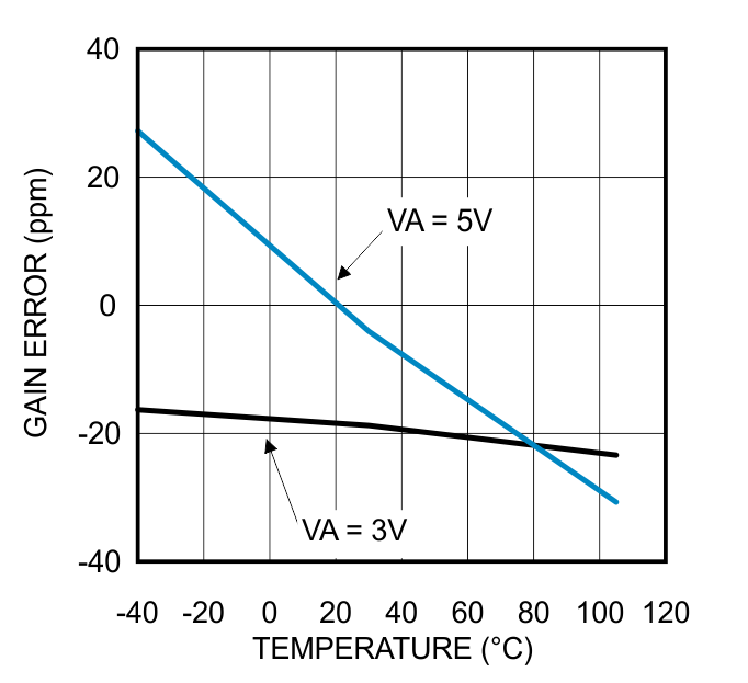 Figure 33. Gain Error vs. Temperature With Calibration
 at Gain = 1
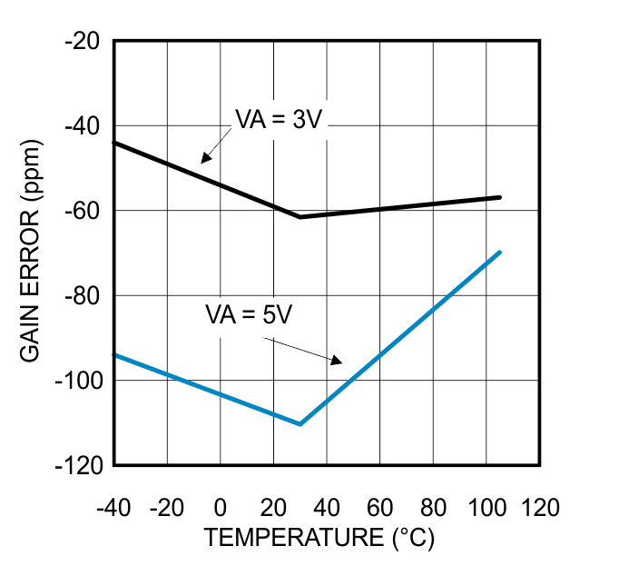 Figure 35. Gain Error vs. Temperature With Calibration
 at Gain = 8
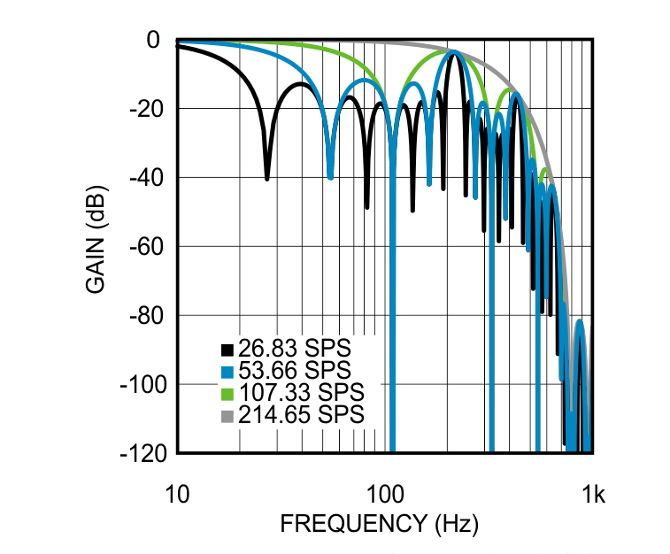 Figure 37. Digital Filter Frequency Response