ZHCS590Q January   2011  – December 2014 LMP90097 , LMP90098 , LMP90099 , LMP90100

PRODUCTION DATA.  

  1. 特性
  2. 应用
  3. 说明
  4. 典型应用电路原理图
  5. 修订历史记录
  6. 说明(续)
  7. Pin Configuration and Functions
  8. Specifications
    1. 8.1  Absolute Maximum Ratings
    2. 8.2  ESD Ratings
    3. 8.3  Recommended Operating Conditions
    4. 8.4  Thermal Information
    5. 8.5  Electrical Characteristics
    6. 8.6  SPI Timing Requirements
    7. 8.7  CBS Setup and Hold Timing Requirements
    8. 8.8  SDI Timing Requirements
    9. 8.9  SDO Timing Requirements
    10. 8.10 Typical Characteristics
  9. Detailed Description
    1. 9.1 Overview
    2. 9.2 Functional Block Diagram
    3. 9.3 Feature Description
      1. 9.3.1 True Continuous Background Calibration
      2. 9.3.2 Continuous Background Sensor Diagnostics
      3. 9.3.3 Flexible Input MUX Channels
      4. 9.3.4 Programmable Gain Amplifiers (FGA and PGA)
      5. 9.3.5 Excitation Current Sources (IB1 and IB2) - LMP90100/LMP90098
      6. 9.3.6 Signal Path
        1. 9.3.6.1 Reference Input (VREF)
        2. 9.3.6.2 Flexible Input MUX (VIN)
        3. 9.3.6.3 Selectable Gains (FGA and PGA)
        4. 9.3.6.4 Buffer (BUFF)
        5. 9.3.6.5 Internal/External CLK Selection
        6. 9.3.6.6 Programmable ODRs
        7. 9.3.6.7 Digital Filter
        8. 9.3.6.8 GPIO (D0-D6)
      7. 9.3.7 Calibration
        1. 9.3.7.1 Background Calibration
          1. 9.3.7.1.1 Types of Background Calibration
          2. 9.3.7.1.2 Using Background Calibration
        2. 9.3.7.2 System Calibration
          1. 9.3.7.2.1 System Calibration Offset Coefficient Determination Mode
          2. 9.3.7.2.2 System Calibration Gain Coefficient Determination Mode
          3. 9.3.7.2.3 Post-Calibration Scaling
      8. 9.3.8 Sensor Interface
        1. 9.3.8.1 IB1 and IB2 - Excitation Currents
        2. 9.3.8.2 Burnout Currents
          1. 9.3.8.2.1 Burnout Current Injection
        3. 9.3.8.3 Sensor Diagnostic Flags
          1. 9.3.8.3.1 SHORT_THLD_FLAG
          2. 9.3.8.3.2 RAILS_FLAG
          3. 9.3.8.3.3 POR_AFT_LST_RD:
          4. 9.3.8.3.4 OFLO_FLAGS
          5. 9.3.8.3.5 SAMPLED_CH
      9. 9.3.9 RESET and RESTART
    4. 9.4 Device Functional Modes
      1. 9.4.1 Power Management
      2. 9.4.2 Channels Scan Mode
        1. 9.4.2.1 ScanMode0: Single-Channel Continuous Conversion
        2. 9.4.2.2 ScanMode1: Multiple-Channels Single Scan
        3. 9.4.2.3 ScanMode2: Multiple-Channels Continuous Scan
        4. 9.4.2.4 ScanMode3: Multiple-Channels Continuous Scan with Burnout Currents
    5. 9.5 Programming
      1. 9.5.1  General Rules
      2. 9.5.2  Serial Digital Interface
      3. 9.5.3  Register Address (ADDR)
      4. 9.5.4  Register Read/Write Protocol
      5. 9.5.5  Streaming
      6. 9.5.6  CSB - Chip Select Bar
      7. 9.5.7  SPI Reset
      8. 9.5.8  DRDYB - Data Ready Bar
      9. 9.5.9  DRDYB Case1: Combining SDO/DRDYB with SDO_DRDYB_DRIVER = 0x00
      10. 9.5.10 DRDYB Case2: Combining SDO/DRDYB with SDO_DRDYB_DRIVER = 0x03
      11. 9.5.11 DRDYB Case3: Routing DRDYB to D6
      12. 9.5.12 Data Only Read Transaction
      13. 9.5.13 Cyclic Redundancy Check (CRC)
      14. 9.5.14 Register Read/Write Examples
        1. 9.5.14.1 Writing To Register Examples
        2. 9.5.14.2 Reading From Register Example
      15. 9.5.15 Streaming Examples
        1. 9.5.15.1 Normal Streaming Example
        2. 9.5.15.2 Controlled Streaming Example
    6. 9.6 Register Maps
  10. 10Application and Implementation
    1. 10.1 Application Information
      1. 10.1.1 Quick Start
      2. 10.1.2 ADC_DOUT Calculation
    2. 10.2 Typical Applications
      1. 10.2.1 3-Wire RTD Using 2 Current Sources
        1. 10.2.1.1 Design Requirements
        2. 10.2.1.2 Detailed Design Procedure
        3. 10.2.1.3 Application Curve
      2. 10.2.2 3-Wire RTD Using 1 Current Source
        1. 10.2.2.1 Design Requirements
        2. 10.2.2.2 Detailed Design Procedure
        3. 10.2.2.3 Application Curve
      3. 10.2.3 Thermocouple with Cold Junction Compensation
        1. 10.2.3.1 Design Requirements
        2. 10.2.3.2 Detailed Design Procedure
      4. 10.2.4 Application Curve
  11. 11Power Supply Recommendations
    1. 11.1 VA and VIO
    2. 11.2 VREF
  12. 12Layout
    1. 12.1 Layout Guidelines
    2. 12.2 Layout Example
  13. 13器件和文档支持
    1. 13.1 器件支持
      1. 13.1.1 器件命名规则
        1. 13.1.1.1 具体定义
    2. 13.2 相关链接
    3. 13.3 商标
    4. 13.4 静电放电警告
    5. 13.5 术语表
  14. 14机械封装和可订购信息

封装选项

机械数据 (封装 | 引脚)
散热焊盘机械数据 (封装 | 引脚)
订购信息

13 器件和文档支持

13.1 器件支持

13.1.1 器件命名规则

13.1.1.1 具体定义

    共模抑制比 (CMRR)

    = 20 LOG(Δ共模输入 / Δ输出偏移)

    共模抑制比

    测量的是对两个输入引脚同相共模信号的抑制能力。 要计算 CMRR,需测得共模输入电压变化时的输出偏移变化。
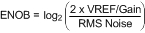
    有效位数 (ENOB) –

    表示转换器与理想 ADC 等效的有效位数量 (ENOB)。 LMP90xxx 的 ENOB 是一项 DC ENOB 规格,而不是使用 FFT 和 SINAD 测得的动态 ENOB。 其计算格式如下:

    Equation 17. 30139513.gif
    增益误差

    是与传递函数理想斜率间的偏差。

    积分非线性 (INL)

    测量的是直线通过输入到输出传递函数的每一个代码的偏差。 这条直线上的任何给定代码的偏差都是从代码值的中心测量的。 使用的是端点拟合方法。 根据电气特性表,该产品的 INL 规定在一个有限范围内。

    负满量程误差

    是输出代码转换到负满量程时的差动输入电压与 (-VREF + 1LSB) 之差。

    负增益误差

    是负满量程误差与偏移误差除以(VREF/增益)之差。
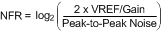
    无噪声分辨率

    是指定转换器噪声位数的一种方法。

    Equation 18. 30139514.gif
    ODR

    输出数据速率。

    偏移误差

    是输出代码从代码 0000h 转换到 0001h 的差分输入电压与 1LSB 之差。

    正满量程误差

    是输出代码转换到正满量程时的差动输入电压与 (VREF – 1LSB) 之差。

    正增益误差

    是正满量程误差与偏移误差除以(VREF/增益)之差。

    电源抑制比 (PSRR)

    测量的是对模拟电源电压变化的抑制能力。 PSRR 计算的是给定电源电压变化量的偏移误差变化比,单位为 dB。

    PSRR

    = 20 LOG (ΔVA / Δ输出偏移)

13.2 相关链接

以下表格列出了快速访问链接。 范围包括技术文档、支持与社区资源、工具和软件,并且可以快速访问样片或购买链接。

13.3 商标

WEBENCH is a registered trademark of Texas Instruments.

All other trademarks are the property of their respective owners.

13.4 静电放电警告

esds-image

这些装置包含有限的内置 ESD 保护。 存储或装卸时,应将导线一起截短或将装置放置于导电泡棉中,以防止 MOS 门极遭受静电损伤。

13.5 术语表

SLYZ022TI 术语表

这份术语表列出并解释术语、首字母缩略词和定义。