ZHCS590Q January   2011  – December 2014 LMP90097 , LMP90098 , LMP90099 , LMP90100

PRODUCTION DATA.  

  1. 特性
  2. 应用
  3. 说明
  4. 典型应用电路原理图
  5. 修订历史记录
  6. 说明(续)
  7. Pin Configuration and Functions
  8. Specifications
    1. 8.1  Absolute Maximum Ratings
    2. 8.2  ESD Ratings
    3. 8.3  Recommended Operating Conditions
    4. 8.4  Thermal Information
    5. 8.5  Electrical Characteristics
    6. 8.6  SPI Timing Requirements
    7. 8.7  CBS Setup and Hold Timing Requirements
    8. 8.8  SDI Timing Requirements
    9. 8.9  SDO Timing Requirements
    10. 8.10 Typical Characteristics
  9. Detailed Description
    1. 9.1 Overview
    2. 9.2 Functional Block Diagram
    3. 9.3 Feature Description
      1. 9.3.1 True Continuous Background Calibration
      2. 9.3.2 Continuous Background Sensor Diagnostics
      3. 9.3.3 Flexible Input MUX Channels
      4. 9.3.4 Programmable Gain Amplifiers (FGA and PGA)
      5. 9.3.5 Excitation Current Sources (IB1 and IB2) - LMP90100/LMP90098
      6. 9.3.6 Signal Path
        1. 9.3.6.1 Reference Input (VREF)
        2. 9.3.6.2 Flexible Input MUX (VIN)
        3. 9.3.6.3 Selectable Gains (FGA and PGA)
        4. 9.3.6.4 Buffer (BUFF)
        5. 9.3.6.5 Internal/External CLK Selection
        6. 9.3.6.6 Programmable ODRs
        7. 9.3.6.7 Digital Filter
        8. 9.3.6.8 GPIO (D0-D6)
      7. 9.3.7 Calibration
        1. 9.3.7.1 Background Calibration
          1. 9.3.7.1.1 Types of Background Calibration
          2. 9.3.7.1.2 Using Background Calibration
        2. 9.3.7.2 System Calibration
          1. 9.3.7.2.1 System Calibration Offset Coefficient Determination Mode
          2. 9.3.7.2.2 System Calibration Gain Coefficient Determination Mode
          3. 9.3.7.2.3 Post-Calibration Scaling
      8. 9.3.8 Sensor Interface
        1. 9.3.8.1 IB1 and IB2 - Excitation Currents
        2. 9.3.8.2 Burnout Currents
          1. 9.3.8.2.1 Burnout Current Injection
        3. 9.3.8.3 Sensor Diagnostic Flags
          1. 9.3.8.3.1 SHORT_THLD_FLAG
          2. 9.3.8.3.2 RAILS_FLAG
          3. 9.3.8.3.3 POR_AFT_LST_RD:
          4. 9.3.8.3.4 OFLO_FLAGS
          5. 9.3.8.3.5 SAMPLED_CH
      9. 9.3.9 RESET and RESTART
    4. 9.4 Device Functional Modes
      1. 9.4.1 Power Management
      2. 9.4.2 Channels Scan Mode
        1. 9.4.2.1 ScanMode0: Single-Channel Continuous Conversion
        2. 9.4.2.2 ScanMode1: Multiple-Channels Single Scan
        3. 9.4.2.3 ScanMode2: Multiple-Channels Continuous Scan
        4. 9.4.2.4 ScanMode3: Multiple-Channels Continuous Scan with Burnout Currents
    5. 9.5 Programming
      1. 9.5.1  General Rules
      2. 9.5.2  Serial Digital Interface
      3. 9.5.3  Register Address (ADDR)
      4. 9.5.4  Register Read/Write Protocol
      5. 9.5.5  Streaming
      6. 9.5.6  CSB - Chip Select Bar
      7. 9.5.7  SPI Reset
      8. 9.5.8  DRDYB - Data Ready Bar
      9. 9.5.9  DRDYB Case1: Combining SDO/DRDYB with SDO_DRDYB_DRIVER = 0x00
      10. 9.5.10 DRDYB Case2: Combining SDO/DRDYB with SDO_DRDYB_DRIVER = 0x03
      11. 9.5.11 DRDYB Case3: Routing DRDYB to D6
      12. 9.5.12 Data Only Read Transaction
      13. 9.5.13 Cyclic Redundancy Check (CRC)
      14. 9.5.14 Register Read/Write Examples
        1. 9.5.14.1 Writing To Register Examples
        2. 9.5.14.2 Reading From Register Example
      15. 9.5.15 Streaming Examples
        1. 9.5.15.1 Normal Streaming Example
        2. 9.5.15.2 Controlled Streaming Example
    6. 9.6 Register Maps
  10. 10Application and Implementation
    1. 10.1 Application Information
      1. 10.1.1 Quick Start
      2. 10.1.2 ADC_DOUT Calculation
    2. 10.2 Typical Applications
      1. 10.2.1 3-Wire RTD Using 2 Current Sources
        1. 10.2.1.1 Design Requirements
        2. 10.2.1.2 Detailed Design Procedure
        3. 10.2.1.3 Application Curve
      2. 10.2.2 3-Wire RTD Using 1 Current Source
        1. 10.2.2.1 Design Requirements
        2. 10.2.2.2 Detailed Design Procedure
        3. 10.2.2.3 Application Curve
      3. 10.2.3 Thermocouple with Cold Junction Compensation
        1. 10.2.3.1 Design Requirements
        2. 10.2.3.2 Detailed Design Procedure
      4. 10.2.4 Application Curve
  11. 11Power Supply Recommendations
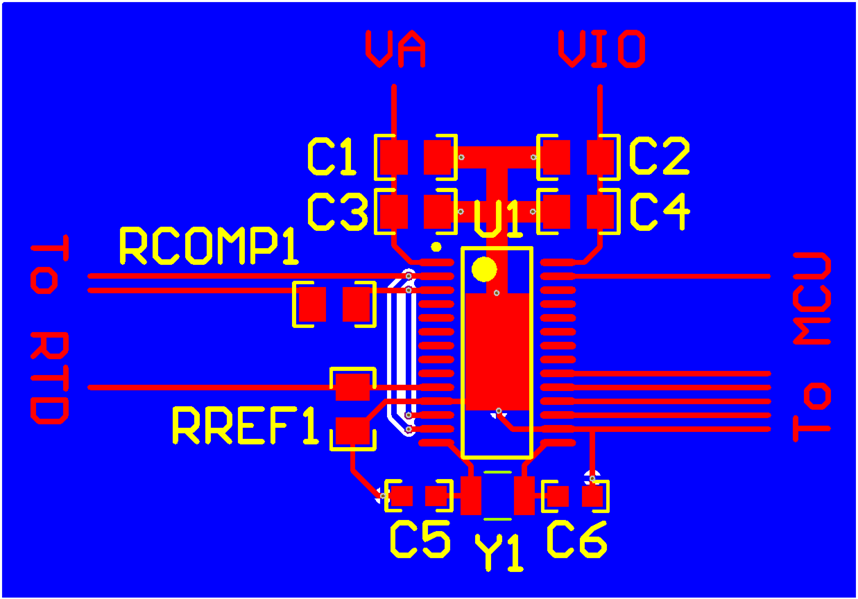
    1. 11.1 VA and VIO
    2. 11.2 VREF
  12. 12Layout
    1. 12.1 Layout Guidelines
    2. 12.2 Layout Example
  13. 13器件和文档支持
    1. 13.1 器件支持
      1. 13.1.1 器件命名规则
        1. 13.1.1.1 具体定义
    2. 13.2 相关链接
    3. 13.3 商标
    4. 13.4 静电放电警告
    5. 13.5 术语表
  14. 14机械封装和可订购信息

封装选项

机械数据 (封装 | 引脚)
散热焊盘机械数据 (封装 | 引脚)
订购信息

12 Layout

12.1 Layout Guidelines

  1. Follow the guidelines in the Power Supply Recommendations section.
  2. Keep analog traces away from digital traces.
  3. Never run an analog and digital trace parallel to each other.
  4. If a digital and analog need to cross each other cross them at a 90° angle.
  5. Use a solid ground plane under the LMP90100.

12.2 Layout Example

The example layout in Figure 80 is for the Typical Application, 3-Wire RTD Using 2 Current Sources shown in Figure 74.

30169798.gifFigure 80. LMP90xxx Sample Layout