ZHCS590Q January   2011  – December 2014 LMP90097 , LMP90098 , LMP90099 , LMP90100

PRODUCTION DATA.  

  1. 特性
  2. 应用
  3. 说明
  4. 典型应用电路原理图
  5. 修订历史记录
  6. 说明(续)
  7. Pin Configuration and Functions
  8. Specifications
    1. 8.1  Absolute Maximum Ratings
    2. 8.2  ESD Ratings
    3. 8.3  Recommended Operating Conditions
    4. 8.4  Thermal Information
    5. 8.5  Electrical Characteristics
    6. 8.6  SPI Timing Requirements
    7. 8.7  CBS Setup and Hold Timing Requirements
    8. 8.8  SDI Timing Requirements
    9. 8.9  SDO Timing Requirements
    10. 8.10 Typical Characteristics
  9. Detailed Description
    1. 9.1 Overview
    2. 9.2 Functional Block Diagram
    3. 9.3 Feature Description
      1. 9.3.1 True Continuous Background Calibration
      2. 9.3.2 Continuous Background Sensor Diagnostics
      3. 9.3.3 Flexible Input MUX Channels
      4. 9.3.4 Programmable Gain Amplifiers (FGA and PGA)
      5. 9.3.5 Excitation Current Sources (IB1 and IB2) - LMP90100/LMP90098
      6. 9.3.6 Signal Path
        1. 9.3.6.1 Reference Input (VREF)
        2. 9.3.6.2 Flexible Input MUX (VIN)
        3. 9.3.6.3 Selectable Gains (FGA and PGA)
        4. 9.3.6.4 Buffer (BUFF)
        5. 9.3.6.5 Internal/External CLK Selection
        6. 9.3.6.6 Programmable ODRs
        7. 9.3.6.7 Digital Filter
        8. 9.3.6.8 GPIO (D0-D6)
      7. 9.3.7 Calibration
        1. 9.3.7.1 Background Calibration
          1. 9.3.7.1.1 Types of Background Calibration
          2. 9.3.7.1.2 Using Background Calibration
        2. 9.3.7.2 System Calibration
          1. 9.3.7.2.1 System Calibration Offset Coefficient Determination Mode
          2. 9.3.7.2.2 System Calibration Gain Coefficient Determination Mode
          3. 9.3.7.2.3 Post-Calibration Scaling
      8. 9.3.8 Sensor Interface
        1. 9.3.8.1 IB1 and IB2 - Excitation Currents
        2. 9.3.8.2 Burnout Currents
          1. 9.3.8.2.1 Burnout Current Injection
        3. 9.3.8.3 Sensor Diagnostic Flags
          1. 9.3.8.3.1 SHORT_THLD_FLAG
          2. 9.3.8.3.2 RAILS_FLAG
          3. 9.3.8.3.3 POR_AFT_LST_RD:
          4. 9.3.8.3.4 OFLO_FLAGS
          5. 9.3.8.3.5 SAMPLED_CH
      9. 9.3.9 RESET and RESTART
    4. 9.4 Device Functional Modes
      1. 9.4.1 Power Management
      2. 9.4.2 Channels Scan Mode
        1. 9.4.2.1 ScanMode0: Single-Channel Continuous Conversion
        2. 9.4.2.2 ScanMode1: Multiple-Channels Single Scan
        3. 9.4.2.3 ScanMode2: Multiple-Channels Continuous Scan
        4. 9.4.2.4 ScanMode3: Multiple-Channels Continuous Scan with Burnout Currents
    5. 9.5 Programming
      1. 9.5.1  General Rules
      2. 9.5.2  Serial Digital Interface
      3. 9.5.3  Register Address (ADDR)
      4. 9.5.4  Register Read/Write Protocol
      5. 9.5.5  Streaming
      6. 9.5.6  CSB - Chip Select Bar
      7. 9.5.7  SPI Reset
      8. 9.5.8  DRDYB - Data Ready Bar
      9. 9.5.9  DRDYB Case1: Combining SDO/DRDYB with SDO_DRDYB_DRIVER = 0x00
      10. 9.5.10 DRDYB Case2: Combining SDO/DRDYB with SDO_DRDYB_DRIVER = 0x03
      11. 9.5.11 DRDYB Case3: Routing DRDYB to D6
      12. 9.5.12 Data Only Read Transaction
      13. 9.5.13 Cyclic Redundancy Check (CRC)
      14. 9.5.14 Register Read/Write Examples
        1. 9.5.14.1 Writing To Register Examples
        2. 9.5.14.2 Reading From Register Example
      15. 9.5.15 Streaming Examples
        1. 9.5.15.1 Normal Streaming Example
        2. 9.5.15.2 Controlled Streaming Example
    6. 9.6 Register Maps
  10. 10Application and Implementation
    1. 10.1 Application Information
      1. 10.1.1 Quick Start
      2. 10.1.2 ADC_DOUT Calculation
    2. 10.2 Typical Applications
      1. 10.2.1 3-Wire RTD Using 2 Current Sources
        1. 10.2.1.1 Design Requirements
        2. 10.2.1.2 Detailed Design Procedure
        3. 10.2.1.3 Application Curve
      2. 10.2.2 3-Wire RTD Using 1 Current Source
        1. 10.2.2.1 Design Requirements
        2. 10.2.2.2 Detailed Design Procedure
        3. 10.2.2.3 Application Curve
      3. 10.2.3 Thermocouple with Cold Junction Compensation
        1. 10.2.3.1 Design Requirements
        2. 10.2.3.2 Detailed Design Procedure
      4. 10.2.4 Application Curve
  11. 11Power Supply Recommendations
    1. 11.1 VA and VIO
    2. 11.2 VREF
  12. 12Layout
    1. 12.1 Layout Guidelines
    2. 12.2 Layout Example
  13. 13器件和文档支持
    1. 13.1 器件支持
      1. 13.1.1 器件命名规则
        1. 13.1.1.1 具体定义
    2. 13.2 相关链接
    3. 13.3 商标
    4. 13.4 静电放电警告
    5. 13.5 术语表
  14. 14机械封装和可订购信息

封装选项

机械数据 (封装 | 引脚)
散热焊盘机械数据 (封装 | 引脚)
订购信息

1 特性

  • 24 位低功耗 Σ-Δ 模数转换器 (ADC)
  • 所有增益上的真连续后台校准
  • 使用期望值编程进行适当的系统校准
  • 低噪声可编程增益(1x 至 128x)
  • 连续后台传感器诊断,可检测开路/短路状态和超范围信号
  • 8 个输出数据速率 (ODR),可在单周期内稳定
  • 两个匹配的激励电流源,100µA 至 1000µA (LMP90100/LMP90098)
  • 4 个差分输入/7 个单端输入 (LMP90100/LMP90099)
  • 2 个差分输入/4 个单端输入 (LMP90098/LMP90097)
  • 7 个通用输入/输出引脚
  • 用于实现低偏移的斩波稳定缓冲器
  • SPI 4/3 线制,采用 CRC 数据链路错误检测
  • ODR
    ≤13.42 SPS 时提供 50Hz 至 60Hz 的线路抑制
  • 每通道独立增益和 ODR 选择
  • 由 WEBENCH® 传感器 AFE 设计工具提供支持
  • 自动通道排序器
  • 主要技术规格
    • ENOB/NFR 多达 21.5/19 位
    • 偏移误差(典型值)8.4nV
    • 增益误差(典型值)7ppm
    • 总体噪声 < 10µV-rms
    • 积分非线性(INL 最大值)满量程范围 (FSR) ± 15ppm
    • 输出数据速率 (ODR) 1.6775 - 214.65 SPS
    • 模拟电压,VA 2.85V 至 5.5V
    • 运行温度范围 -40℃ 至 125℃
    • 采用 28 引脚散热薄型小外形尺寸 (HTSSOP) 外露垫封装

2 应用

  • 温度和压力发送器
  • 应变仪接口
  • 工业过程控制

3 说明

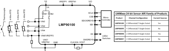
LMP90xxx 是一款高度集成的多通道低功耗 24 位传感器 AFE。 该器件配有一个精密的 24 位 Σ-Δ 模数转换器 (ADC),一个低噪声可编程增益放大器以及一个全差动高阻抗模拟输入复用器。 一个真连续后台校准特性可在所有增益和输出数据速率上实现校准而又不会中断信号路径。 后台校准特性在温度和时间范围内从根本上消除了增益和偏移误差,从而在不损失速度和功耗的情况下提供测量精度。

器件信息(1)

器件型号 封装 封装尺寸(标称值)
LMP90097 HTSSOP (28) 9.70 mm x 4.40 mm
LMP90098
LMP90099
LMP90100
  1. 如需了解所有可用封装,请见数据表末尾的可订购产品附录。

4 典型应用电路原理图

30139574.gif