SNOSB28G August 2010 – November 2014 LMP8640 , LMP8640-Q1 , LMP8640HV
PRODUCTION DATA.
- 1 Features
- 2 Applications
- 3 Description
- 4 Revision History
- 5 Device Comparison Table
- 6 Pin Configuration and Functions
-
7 Specifications
- 7.1 Absolute Maximum Ratings
- 7.2 Handling Ratings - LMP8640, LMP8640HV
- 7.3 Handling Ratings - LMP8640-Q1
- 7.4 Recommended Operating Conditions
- 7.5 Thermal Information
- 7.6 Electrical Characteristics 2.7 V
- 7.7 Electrical Characteristics 5 V
- 7.8 Electrical Characteristics 12 V
- 7.9 Typical Characteristics
- 8 Detailed Description
- 9 Application and Implementation
- 10Power Supply Recommendations
- 11Layout
- 12Device and Documentation Support
- 13Mechanical, Packaging, and Orderable Information
11 Layout
11.1 Layout Guidelines
- Use 4-wire (Kelvin) connections to the sense resistor. Connect to the resistor at a point that is not within a direct high-current path (See Figure 29).
- Do not "share" part of the sense trace path with the load current.
- Maintain proper clearance and spacings around the input traces, as they may be at a higher voltage (up to 76 V) than the surrounding traces and planes.
- Input traces from the sense resistor pads should follow the same path, be spaced tightly together, and ideally on the same copper layer.
- Vias used in the input traces should be of continuous plated copper to avoid creating thermocouples.
- Avoid routing inputs through jumpers and connectors. Even the best connectors introduce thermal errors ("thermocouples"). Each input trace should have the same number of "thermocouples" if they cannot be avoided.
- Keep the amplifier away from heat generating devices. The copper-solder-lead junction on the input pins will form a thermocouple. The copper mass should be equal on both input pins.
- Avoid temperature gradients across the input pins. Input pins should be equal distance to the heat source.
- Place the LMP8640 in the most temperature-stable area possible and away from high-velocity air flows. It is better to carefully extend the input traces than to place the amplifier in a less-than-ideal environment.
- Give the sense resistor as much copper trace area as possible to dissipate heat as the resistor value will change slightly with temperature. Also see the resistor manufacturers datasheet or application notes for further layout guidelines.
- The power-supply bypass capacitor should be placed as closely as possible to the supply and ground terminals. The recommended value of this bypass capacitor is 0.1 μF. Additional decoupling capacitance can be added to compensate for noisy or high-impedance power supplies.
11.2 Layout Example
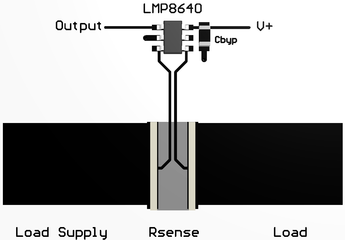 Figure 29. Layout Example - Kelvin Connection to a Two-Terminal Resistor
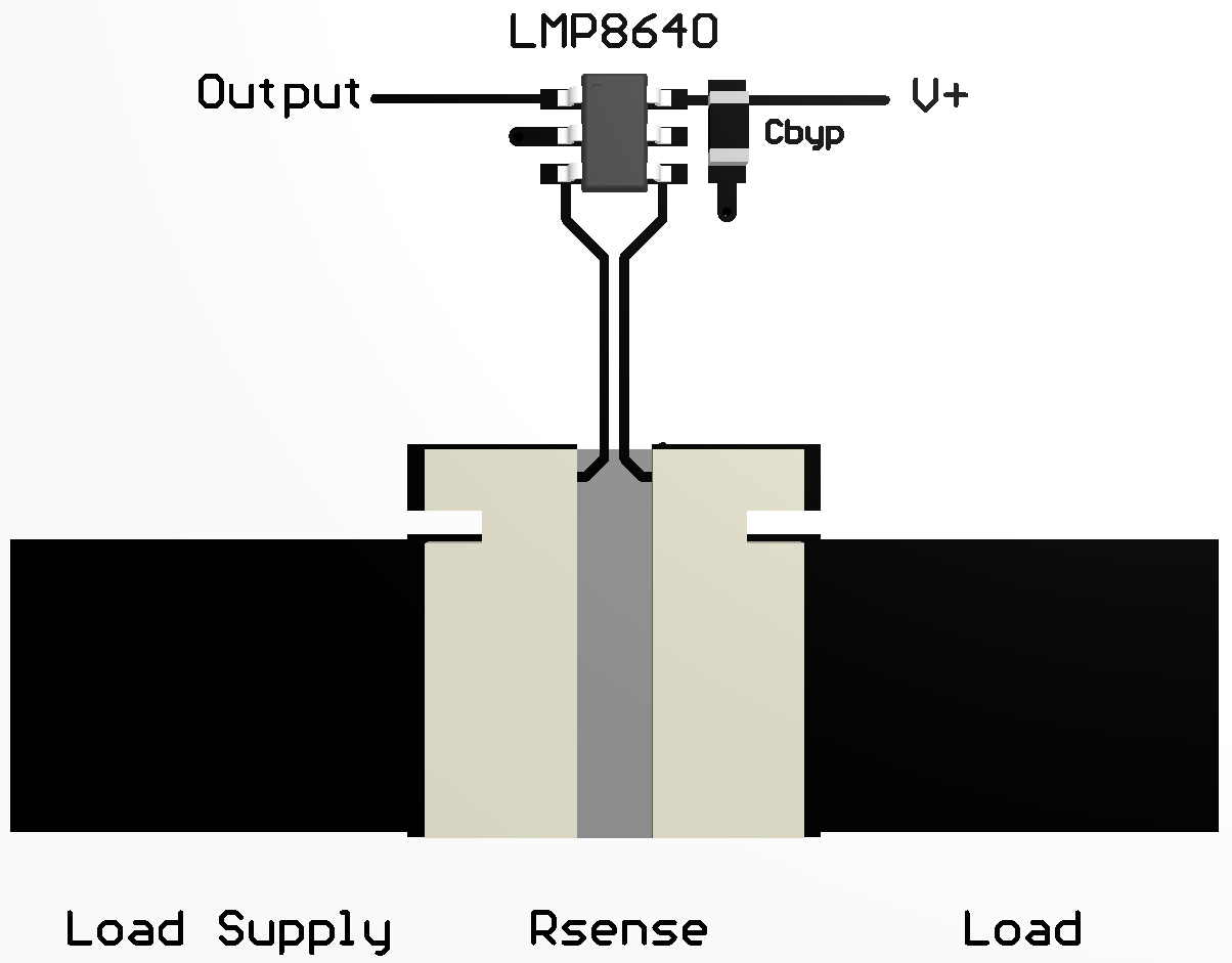 Figure 30. Layout Example - Four-Wire (Kelvin) Resistor Connection