SNOSB28G August 2010 – November 2014 LMP8640 , LMP8640-Q1 , LMP8640HV
PRODUCTION DATA.
- 1 Features
- 2 Applications
- 3 Description
- 4 Revision History
- 5 Device Comparison Table
- 6 Pin Configuration and Functions
-
7 Specifications
- 7.1 Absolute Maximum Ratings
- 7.2 Handling Ratings - LMP8640, LMP8640HV
- 7.3 Handling Ratings - LMP8640-Q1
- 7.4 Recommended Operating Conditions
- 7.5 Thermal Information
- 7.6 Electrical Characteristics 2.7 V
- 7.7 Electrical Characteristics 5 V
- 7.8 Electrical Characteristics 12 V
- 7.9 Typical Characteristics
- 8 Detailed Description
- 9 Application and Implementation
- 10Power Supply Recommendations
- 11Layout
- 12Device and Documentation Support
- 13Mechanical, Packaging, and Orderable Information
9 Application and Implementation
NOTE
Information in the following applications sections is not part of the TI component specification, and TI does not warrant its accuracy or completeness. TI’s customers are responsible for determining suitability of components for their purposes. Customers should validate and test their design implementation to confirm system functionality.
9.1 Application Information
The LMP8640x amplifies the voltage developed across a current-sensing resistor.
9.2 Typical Application
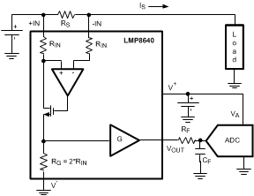 Figure 27. Typical Application Example
9.2.1 Design Requirements
In this example, a current monitor application is required to measure the current into a load (peak current 10 A) with a resolution of 10 mA and 0.5% of accuracy.
The 10bit analog to digital converter accepts a max input voltage of 4.1 V. In order to not burn too much power on the shunt resistor, it needs to be less than 10 mΩ. Table 1 below summarizes the other design conditions.
Table 1. Example Design Requirements
| WORKING CONDITION | VALUE | |
|---|---|---|
| MIN | MAX | |
| Supply Voltage | 5 V | 5.5 V |
| Common mode Voltage | 48 V | 70 V |
| Temperature | 0°C | 70°C |
| Signal BW | 50 kHz | |
9.2.2 Design Procedure
9.2.2.1 First Step – LMP8640 or LMP8640HV Selection
The required common mode voltage of the application implies that the right choice is the LMP8640HV (High common mode voltage up tp 76 V).
9.2.2.2 Second Step – Gain Option Selection
We can choose between three gain option (20 V/V, 50 V/V, 100 V/V). Considering the max input voltage of the ADC (4.1 V) , the max Sense voltage across the shunt resistor is evaluated according the following formula:
hence the max VSENSE will be 205 mV, 82 mV, 41 mV respectively. The shunt resistor are then evaluated considering the maximum monitored current :
For each gain option the max shunt resistors are the following : 20.5 mΩ, 8.2 mΩ, 4.1 mΩ respectively.
One of the project constraints requires RS<10 mΩ, it means that the 20.5 mΩ will be discarded and hence the 50 V/V and 100 V/V gain options are still in play.
9.2.2.3 Third Step – Shunt Resistor Selection
At this point an error budget calculation, considering the calibration of the Gain, Offset, CMRR, and PSRR, helps in the selection of the shunt resistor. In the table below the contribution of each error source is calculated considering the values of the Electrical Characteristics table at 5 V supply.
Table 2. Resolution Calculation
| ERROR SOURCE | RS = 4.1 mΩ | RS = 8.1 mΩ |
|---|---|---|
| CMRR calibrated at mid VCM range | 77.9 µV | 77.9 µV |
| PSRR calibrated at 5 V | 8.9 µV | 8.9 µV |
| Total error (squared sum of contribution) | 78 µV | 78 µV |
| Resolution (Total error / RS) | 19.2 mA | 9.6 mA |
Table 3. Accuracy Calculation
| ERROR SOURCE | RS = 4.1 mΩ | RS = 8.1 mΩ |
|---|---|---|
| Tc Vos | 182 µV | 182 µV |
| Nosie | 216 µV | 216 µV |
| Gain drift | 75.2 µV | 151 µV |
| Total error (squared sum of contribution) | 293 µV | 320 µV |
| Accuracy 100*(Max_VSENSE / Total Error) | 0.7% | 0.4% |
From the tables above is clear that the 8.2 mΩ shunt resistor allows the respect of the project's constraints. The power burned on the Shunt is 820 mW at 10 A.
9.2.3 Application Performance Plot
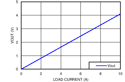 Figure 28. Application Example Results using 8.2 mΩ Resistor