SNOSB28G August 2010 – November 2014 LMP8640 , LMP8640-Q1 , LMP8640HV
PRODUCTION DATA.
- 1 Features
- 2 Applications
- 3 Description
- 4 Revision History
- 5 Device Comparison Table
- 6 Pin Configuration and Functions
-
7 Specifications
- 7.1 Absolute Maximum Ratings
- 7.2 Handling Ratings - LMP8640, LMP8640HV
- 7.3 Handling Ratings - LMP8640-Q1
- 7.4 Recommended Operating Conditions
- 7.5 Thermal Information
- 7.6 Electrical Characteristics 2.7 V
- 7.7 Electrical Characteristics 5 V
- 7.8 Electrical Characteristics 12 V
- 7.9 Typical Characteristics
- 8 Detailed Description
- 9 Application and Implementation
- 10Power Supply Recommendations
- 11Layout
- 12Device and Documentation Support
- 13Mechanical, Packaging, and Orderable Information
8 Detailed Description
8.1 Overview
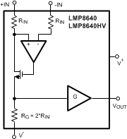
The LMP8640 and LMP8640HV are single supply high side current sense amplifiers with a fixed gain of 20 V/V, 50 V/V, 100 V/V and a common mode voltage range of -2 V to 42 V (LMP8640-x) or -2 V to 76 V (LMP8640HV-x) with a buffered voltage output.
8.2 Functional Block Diagram
8.3 Feature Description
As seen in Figure 25, the current flowing through sense resistor RS develops a voltage drop equal to VSENSE across RS. The voltage at the -IN pin will now be less than +IN by an amount proportional to the VSENSE voltage.
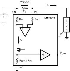 Figure 25. Simple Current Monitor
The low bias currents of the error amplifier cause little voltage drop through RIN-, so the negative input of the internal error amplifier is at essentially the same potential as the -IN input. The RIN resistors are 5 KΩ each.
The error amplifier will detect this voltage error between it's inputs and drive the MOSFET gate to conduct more current, increasing the voltage drop across RIN+, until the servo amplifiers positive input matches the negative input. At this point, the voltage drop across RIN+ now matches VSENSE.
IG, a current proportional to IS, will flow according to the following relation:
IG also flows through the internal gain resistor RG developing a voltage drop equal to:
where G=RG/RIN = 10 V/V, 25 V/V or 50 V/V, according to the gain option selected.
The voltage on RG is then amplified by a gain of 2 by the output gain stage to create the final overall gain of x20, x50 and x100. The output stage has a low impedance drive allowing the LMP8640 to easily interface with other IC's (ADC, Mux, µC…). No external buffering is required.
8.3.1 Selection of Sense Resistor
The value chosen for the shunt resistor, RS, depends on the application. It plays a big role in a current sensing system and must be chosen with care. The selection of the shunt resistor needs to take in account the tradeoffs in small-signal accuracy, the power dissipated and the voltage loss across the shunt itself.
In applications where a small current is sensed, a bigger value of RS is selected to minimize the error in the proportional output voltage. Higher resistor value improves the signal-to-noise ratio (SNR) at the input of the current sense amplifier and hence gives a more accurate output.
Similarly when high current is sensed, the power losses in RS can be significant so a smaller value of RS is desired. In this condition it is also required to take in account also the power rating of RS resistor. The low input offset of the LMP8640 allows the use of small sense resistors to reduce power dissipation still providing a good input dynamic range. The input dynamic range is the ratio between the maximum signal that can be measured and the minimum signal that can be detected, where usually the input offset is the principal limiting factor.
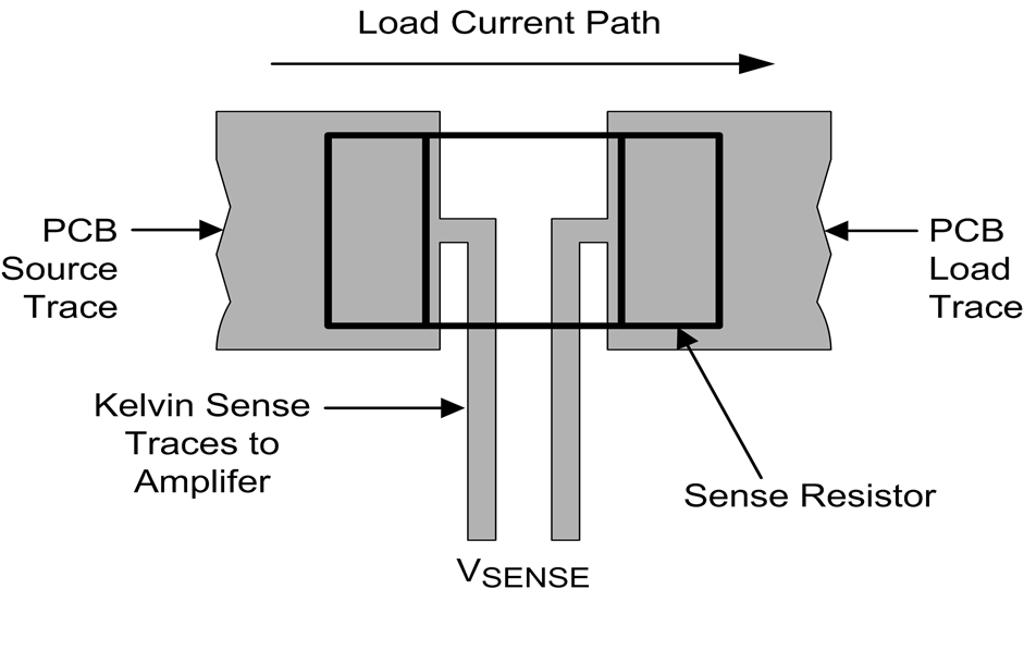 Figure 26. Example of a Kelvin (4-Wire) Connection to a Two-Terminal Resistor
The amplifier inputs should be directly connected to the sense resistor pads using “Kelvin” or “4-wire” connection techniques. The paths of the input traces should be identical, including connectors and vias, so that these errors will be equal and cancel.
8.3.1.1 Resistor Power Rating and Thermal Issues
The power dissipated by the sense resistor can be calculated from:
where
- PD is the power dissipated by the resistor in Watts
- IMAX is the maximum load current in Amps
- RS is the sense resistor value in ohms.
The resistor must be rated for more than the expected maximum power (PD), with margin for temperature derating. Be sure to observe any power derating curves provided by the resistor manufacturer.
Running the resistor at higher temperatures will also affect the accuracy. As the resistor heats up, the resistance generally goes up, which will cause a change in the measurement. The sense resistor should have as much heat-sinking as possible to remove this heat through the use of heatsinks or large copper areas coupled to the resistor pads. A reading drifting slightly after turn-on can usually be traced back to sense resistor heating.
8.3.1.2 Using PCB Trace as a Sense Resistor
While it may be tempting to use the resistance of a known area of PCB trace or copper area as a sense resistor, it is not recommended for precision measurements.
The tempco of copper is typically 3300-4000ppm/°K (0.33% to 0.4% per °C), which can vary with PCB processes.
A typical surface mount sense resistor temperature coefficient (tempco) is in the 50ppm to 500ppm per °C range offering more measurement consistency and accuracy over the copper trace. Special low tempco resistors are available in the 0.1 to 50ppm range, but at a much higher cost.
8.3.2 Sense Line Inputs
The sense lines should be connected to a point on the resistor that is not shared with the main current path, as shown in Figure 26 above. For lowest drift, the amplifier should be mounted away from any heat generating devices, which may include the sense resistor. The traces should be one continuous trace of copper from the sense resistor pad to the amplifier input pin pad, and ideally on the same copper layer with minimal vias or connectors. This can be important around the sense resistor if it is generating any significant heat gradients. Vias in the sense lines should be formed from continuous plated copper and routing through connectors should be avoided. It is better to extend the sense lines than to place the amplifier in a hostile environment.
To minimize noise pickup and thermal errors, the input traces should be treated like a high-speed differential signal pair and routed tightly together with a direct path to the input pins on the same copper layer. They do not need to be "impedance matched", but should follow the same matching rules about vias, spacing and equal lengths. The input traces should be run away from noise sources, such as digital lines, switching supplies or motor drive lines. Remember that these input traces can contain high voltage, and should have the appropriate trace routing clearances to other traces and layers. Since the sense traces only carry the amplifier bias current (typically about 12µA per input at room temp), the connecting input traces can be thin traces running close together. This can help with routing or creating the required spacings.
It should also be noted that, due to the nature of the device topology, the positive input bias current will vary with VSENSE with an extra current approximately equivalent to VSENSE / 5 kΩ on top of the typical 12 uA bias current. The negative input bias current is not in the feedback path and will not change over VSENSE. High or miss-matched source impedances should be avoided as this imbalance will create an additional error over input voltage.
8.3.3 Effects of Series Resistance on Sense Lines
Because the input stage uses precision 5 KΩ resistors internally to convert the voltage on the input pin to a current, any resistance added in series with the input pins will change this resistance, and thus alter the gain.
If a resistance is added in series with an input, the gain of that input will not track that of the other input, causing a constant gain error.
It is not recommended to use external resistance to alter the gain, as external resistors will not have the same thermal matching as the internal thin film resistors. Any added resistance will severely degrade the offset and CMRR specifications. It is recommended that the total trace resistance be less than 10 ohms.
If resistors are purposely added for filtering, resistance should be added equally to both inputs and the user should be aware that the gain will change slightly.
8.4 Device Functional Modes
8.4.1 Bias Current at Low Common Mode Voltage
At common mode voltages below +2 V, the input bias current starts to reverse and crosses through zero at about +1.8 V. This can be seen in the Input Bias Current graphs in Figure 9 through Figure 11. Negative currents on the graph show curent flow out of the input and into the load. The graphs show the current for each input, so the actual "bias" current will be twice graph value. This total current could be as high as 1mA, depending on the point of equilibrium.
While this will not affect the vast majority of applications, it may cause MOSFET switched designs with non-linear loads (like LED's or diode-isolated loads) to "float" above ground where the load leakage and bias currents attain equilibrium. A small resistor to ground (on the load supply side) can bleed-off this current.
8.4.2 Applying Input Voltage with No Supply Voltage
The full specified input common mode voltage range may be applied to the inputs while the LMP8640 power is off (V+ = 0 V). When the LMP8640 is powered off, the RIN resistors are disconnected internally by MOSFETS and the leakage currents are very low (sub uA).
The 6 V input differential limit still applies, so at no time should the two inputs be more than 6 V apart. There are also Zener clamps on the inputs to ground, so do not exceed the input limits specified in the Absolute Maximum Ratings.
8.4.3 Driving an ADC
The input stage of an Analog to Digital converter can be modeled with a resistor and a capacitance to ground. So if the voltage source doesn't have a low impedance, an error in amplitude measurement will occur. In this case, a buffer is needed to drive the ADC. The LMP8640 has an internal output buffer able to directly drive a capacitive load up to 30 pF, or, the input stage of an ADC. It is recommended that an external low pass RC filter be added to the output of the LMP8640 to reduce the noise and limit the bandwidth of the current sense measurement.
If the supply voltage of the LMP8640 is higher than the ADC supply voltage, care should be taken to prevent the LMP8640 output from over-driving the ADC input.
This can be accomplished with a series resistance (which should be present when driving a ADC) and a clamping diode to the ADC's power supply. The diode will clamp the ADC input to a safe level. Do not completely rely on a calculated maximum output voltage. Transients or fault conditions outside the normal conditions area can cause the output to swing to a higher than expected voltage.