ZHCSDN0E March   1999  – February 2017 LMP8480 , LMP8481

PRODUCTION DATA.  

  1. 特性
  2. 应用
  3. 说明
  4. 修订历史记录
  5. Device Comparison Table
  6. Pin Configuration and Functions
  7. Specifications
    1. 7.1 Absolute Maximum Ratings
    2. 7.2 ESD Ratings
    3. 7.3 Recommended Operating Conditions
    4. 7.4 Thermal Information
    5. 7.5 Electrical Characteristics
    6. 7.6 Typical Characteristics
  8. Detailed Description
    1. 8.1 Overview
      1. 8.1.1 Theory of Operation
    2. 8.2 Functional Block Diagrams
    3. 8.3 Feature Description
      1. 8.3.1  Basic Connections
      2. 8.3.2  Selection of the Sense Resistor
      3. 8.3.3  Using PCB Traces as Sense Resistors
      4. 8.3.4  VREFA and VREFB Pins (LMP8481 Only)
        1. 8.3.4.1 One-to-One (1:1) Reference Input
        2. 8.3.4.2 Setting Output to One-Half VCC or external VREF
      5. 8.3.5  Reference Input Voltage Limits (LMP8481 Only)
      6. 8.3.6  Low-Side Current Sensing
      7. 8.3.7  Input Series Resistance
      8. 8.3.8  Minimum Output Voltage
      9. 8.3.9  Swinging Output Below Ground
      10. 8.3.10 Maximum Output Voltage
    4. 8.4 Device Functional Modes
      1. 8.4.1 Unidirectional vs Bidirectional Operation
  9. Application and Implementation
    1. 9.1 Application Information
      1. 9.1.1 Input Common-Mode and Differential Voltage Range
    2. 9.2 Typical Applications
      1. 9.2.1 Unidirectional Application With the LMP8480
        1. 9.2.1.1 Design Requirements
        2. 9.2.1.2 Detailed Design Procedure
        3. 9.2.1.3 Application Curve
      2. 9.2.2 Bidirectional Current Sensing Using the LMP8481
        1. 9.2.2.1 Design Requirements
        2. 9.2.2.2 Detailed Design Procedure
        3. 9.2.2.3 Application Curve
      3. 9.2.3 Typical Application With a Resistive Divider
  10. 10Power Supply Recommendations
    1. 10.1 Power Supply Decoupling
  11. 11Layout
    1. 11.1 Layout Guidelines
    2. 11.2 Layout Example
  12. 12器件和文档支持
    1. 12.1 器件支持
      1. 12.1.1 开发支持
    2. 12.2 相关链接
    3. 12.3 接收文档更新通知
    4. 12.4 社区资源
    5. 12.5 商标
    6. 12.6 静电放电警告
    7. 12.7 Glossary
  13. 13机械、封装和可订购信息

封装选项

机械数据 (封装 | 引脚)
散热焊盘机械数据 (封装 | 引脚)
订购信息

Pin Configuration and Functions

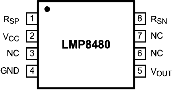
LMP8480 VSSOP Package
8 Pins
Top View
LMP8480 LMP8481 30191520.png
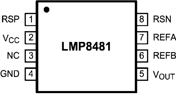
LMP8481 VSSOP Package
8 Pins
Top View
LMP8480 LMP8481 30191521.png

Pin Functions

PIN I/O DESCRIPTION
NO. NAME
1 RSP I Positive current sense input
2 VCC P Positive supply voltage
3 NC No connection – not internally connected
4 GND P Ground
5 VOUT O Output
6 NC or REFB I LMP8480: no connection LMP8481: reference voltage “B” input
7 NC or REFA I LMP8480: no connection LMP8481: reference voltage “A” input
8 RSN I Negative current sense input