ZHCSDA5F June 2012 – February 2015 LMH6881
PRODUCTION DATA.
5 Pin Configuration and Functions
RTW Package
24-Pins WQFN
Top View
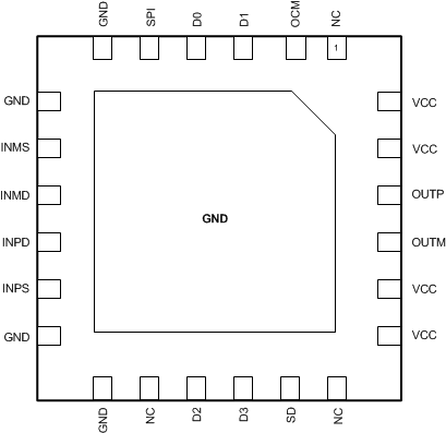
Pin Functions
| PIN | TYPE | DESCRIPTION | |
|---|---|---|---|
| NO. | NAME | ||
| 1 | NC | — | |
| 2 | OCM | I | Output Common Mode, gain of 2 |
| 3 | D1, SDI | I | Parallel mode = Logic control signal, position 1 or weight 21
SPI mode = serial data in (SDI) |
| 4 | D0, SDO | I/O | Parallel mode = Logic control signal, position 0 or weight 20
SPI mode = serial data out (SDO) |
| 5 | SPI | I | Serial mode control |
| 6 | GND | I/O | Ground |
| 7 | GND | I/O | Ground |
| 8 | INMS | I | Amplifier single-ended input minus swing (negative) |
| 9 | INMD | I | Amplifier differential input minus swing (negative) |
| 10 | INPD | I | Amplifier differential input plus swing (positive) |
| 11 | INPS | I | Amplifier single-ended input plus swing (positive) |
| 12 | GND | I/O | Ground |
| 13 | GND | I/O | Ground |
| 14 | NC | — | |
| 15 | D2 | I | Parallel mode = Logic control signal, position 2 or weight 22 SPI mode = serial clock (CLK) |
| 16 | D3 | I | Parallel mode = Logic control signal, position 3 or weight 23 SPI mode = chip select (CS) |
| 17 | SD | I | Device Shutdown |
| 18 | NC | — | |
| 19 | VCC | I/O | Power supply nominal value of 5 V |
| 20 | VCC | I/O | Power supply nominal value of 5 V |
| 21 | OUTM | O | Amplifier output minus (negative) |
| 22 | OUTP | O | Amplifier output plus (positive) |
| 23 | VCC | I/O | Power supply nominal value of 5 V |
| 24 | VCC | I/O | Power supply nominal value of 5 V |
Pin Descriptions
| NO. | SYMBOL | PIN CATEGORY | DESCRIPTION |
|---|---|---|---|
| ANALOG I/O | |||
| 9,10 | INPD, INMD | Analog Input | Differential inputs 100 Ω |
| 8, 11 | INPS, INMS | Analog Input | Single-ended inputs 50 Ω |
| 21, 22 | OUTP, OUTM | Analog Output | Differential outputs, low impedance |
| POWER | |||
| 6, 7, 12, 13 | GND | Ground | Ground pins. Connect to low impedance ground plane. All pin voltages are specified with respect to the voltage on these pins. The exposed thermal pad is internally bonded to the ground pins. |
| 19, 20, 23, 24 | VCC | Power | Power supply pins. Valid power supply range is 4.75 V to 5.25 V. |
| Exposed Center Pad | Thermal/ Ground | Thermal management/ Ground | |
| DIGITAL INPUTS | |||
| 5 | SPI | Digital Input | 0 = Parallel Mode, 1 = Serial Mode |
| PARALLEL MODE DIGITAL PINS, SPI = LOGIC LOW | |||
| 3, 4, 15, 16 | D0, D1, D2, D3 | Digital Input | Attenuator control |
| 17 | SD | Digital Input | Shutdown 0 = amp on, 1 = amp off |
| SERIAL MODE DIGITAL PINS, SPI= LOGIC HIGH, SPI COMPATIBLE | |||
| 4 | SDO | Digital Output - Open Emitter | Serial Data Output (Requires external bias.) |
| 3 | SDI | Digital Input | Serial Data In |
| 16 | CS | Digital Input | Chip Select (active low) |
| 15 | CLK | Digital Input | Clock |