SNOSB30P October 2008 – January 2015 LMH6554
PRODUCTION DATA.
- 1 Features
- 2 Applications
- 3 Description
- 4 Typical Application Schematic
- 5 Revision History
- 6 Pin Configuration and Functions
- 7 Specifications
- 8 Detailed Description
- 9 Application and Implementation
- 10Power Supply Recommendations
- 11Layout
- 12Device and Documentation Support
- 13Mechanical, Packaging, and Orderable Information
6 Pin Configuration and Functions
NHJ Package
14 Pins
Top View
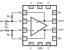
Pin Functions
| PIN | I/O | DESCRIPTION | |
|---|---|---|---|
| NAME | NO. | ||
| -FB | 7 | O | Feedback from -OUT |
| +FB | 4 | O | Feedback from +OUT |
| +IN | 6 | I | Positive Input |
| -IN | 5 | I | Negative Input |
| NC | 11 | — | No Connection |
| NC | 14 | — | No Connection |
| -OUT | 12 | O | Negative Output |
| +OUT | 13 | O | Positive Output |
| VCM | 2 | I | Output Common Mode Voltage |
| VEN | 9 | I | Enable |
| V- | 3 | P | Negative Supply |
| V- | 8 | P | Negative Supply |
| V+ | 1 | P | Positive Supply |
| V+ | 10 | P | Positive Supply |