SNOSB30P October 2008 – January 2015 LMH6554
PRODUCTION DATA.
- 1 Features
- 2 Applications
- 3 Description
- 4 Typical Application Schematic
- 5 Revision History
- 6 Pin Configuration and Functions
- 7 Specifications
- 8 Detailed Description
- 9 Application and Implementation
- 10Power Supply Recommendations
- 11Layout
- 12Device and Documentation Support
- 13Mechanical, Packaging, and Orderable Information
9 Application and Implementation
NOTE
Information in the following applications sections is not part of the TI component specification, and TI does not warrant its accuracy or completeness. TI’s customers are responsible for determining suitability of components for their purposes. Customers should validate and test their design implementation to confirm system functionality.
9.1 Application Information
The LMH6554 is a fully differential, current feedback amplifier with integrated output common mode control, designed to provide low distortion amplification to wide bandwidth differential signals. The common mode feedback circuit sets the output common mode voltage independent of the input common mode, as well as forcing the V+ and V− outputs to be equal in magnitude and opposite in phase, even when only one of the inputs is driven as in single to differential conversion.
The proprietary current feedback architecture of the LMH6554 offers gain and bandwidth independence with exceptional gain flatness and noise performance, even at high values of gain, simply with the appropriate choice of RF1 and RF2. Generally RF1 is set equal to RF2, and RG1 equal to RG2, so that the gain is set by the ratio RF/RG. Matching of these resistors greatly affects CMRR, DC offset error, and output balance. A maximum of 0.1% tolerance resistors are recommended for optimal performance, and the amplifier is internally compensated to operate with optimum gain flatness with RF value of 200 Ω depending on PCB layout, and load resistance.
The output common mode voltage is set by the VCM pin with a fixed gain of 1 V/V. This pin should be driven by a low impedance reference and should be bypassed to ground with a 0.1-µF ceramic capacitor. Any unwanted signal coupling into the VCM pin will be passed along to the outputs, reducing the performance of the amplifier.
The LMH6554 can be configured to operate on a single 5-V supply connected to V+ with V- grounded or configured for a split supply operation with V+ = +2.5 V and V− = −2.5 V. Operation on a single 5-V supply, depending on gain, is limited by the input common mode range; therefore, AC coupling may be required. Split supplies will allow much less restricted AC and DC coupled operation with optimum distortion performance.
9.2 Typical Applications
9.2.1 Single-Ended Input to Differential Output Operation
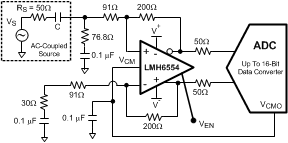 Figure 25. Single-Ended Input to Differential Output Schematic
9.2.1.1 Design Requirements
One typical application for the LMH6554 is to drive an ADC as shown in Figure 25. The following design is a single-ended to differential circuit with an input impedance of 50 Ω and an output impedance of 100 Ω. The VCM voltage of the amplifier needs to be set to the same voltage as the ADC reference voltage, which is typically 1.2 V. Figure 27 shows the design equations required to set the external resistor values. This design also requires a gain of 2 and -96 dBc THD at 75 MHz.
9.2.1.2 Detailed Design Procedure
To match the input impedance of the circuit in Figure 27 to a specified source resistance, RS, requries that RT || RIN = RS. The equations governing RIN and AV for single-to-differential operation are also provided in Figure 27. These equations, along with the source matching condition, must be solved iteratively to achieve the desired gain with the proper input termination. Component values for several common gain configuration in a 50 Ω environment are given in Table 1.
9.2.1.2.1 Enable / Disable Operation
The LMH6554 is equipped with an enable pin (VEN) to reduce power consumption when not in use. The VEN pin, when not driven, floats high (on). When the VEN pin is pulled low, the amplifier is disabled and the amplifier output stage goes into a high impedance state so the feedback and gain set resistors determine the output impedance of the circuit. For this reason input to output isolation will be poor in the disabled state and the part is not recommended in multiplexed applications where outputs are all tied together.
With a 5V difference between V+ and V-, the VEN threshold is ½ way between the supplies (e.g. 2.5V with 5V single supply) as shown in Figure 26. R2 ensures active (enable) mode with VEN floating, and R1 provides input current limiting. VEN also has ESD diodes to either supply.
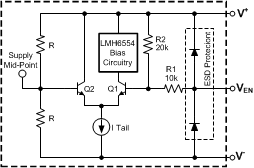 Figure 26. Enable Block Diagram
9.2.1.2.2 Single-Ended Input to Differential Output Operation
In many applications, it is required to drive a differential input ADC from a single ended source. Traditionally, transformers have been used to provide single to differential conversion, but these are inherently bandpass by nature and cannot be used for DC coupled applications. The LMH6554 provides excellent performance as a single-ended input to differential output converter down to DC. Figure 27 shows a typical application circuit where an LMH6554 is used to produce a balanced differential output signal from a single ended source.
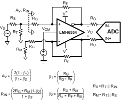 Figure 27. Single-Ended Input with Differential Output
When using the LMH6554 in single-to-differential mode, the complimentary output is forced to a phase inverted replica of the driven output by the common mode feedback circuit as opposed to being driven by its own complimentary input. Consequently, as the driven input changes, the common mode feedback action results in a varying common mode voltage at the amplifier's inputs, proportional to the driving signal. Due to the non-ideal common mode rejection of the amplifier's input stage, a small common mode signal appears at the outputs which is superimposed on the differential output signal. The ratio of the change in output common mode voltage to output differential voltage is commonly referred to as output balance error. The output balance error response of the LMH6554 over frequency is shown in the Typical Performance Characteristics VS = ±2.5 V.
To match the input impedance of the circuit in Figure 27 to a specified source resistance, RS, requries that RT || RIN = RS. The equations governing RIN and AV for single-to-differential operation are also provide in Figure 27. These equations, along with the source matching condition, must be solved iteratively to achieve the desired gain with the proper input termination. Component values for several common gain configuration in a 50Ω environment are given in Table 1.
Table 1. Gain Component Values for 50 Ω System
| GAIN | RF | RG | RT | RM |
|---|---|---|---|---|
| 0dB | 200Ω | 191Ω | 62Ω | 27.7Ω |
| 6dB | 200Ω | 91Ω | 76.8Ω | 30.3Ω |
| 12dB | 200Ω | 35.7Ω | 147Ω | 37.3Ω |
9.2.1.2.3 Driving Capacitive Loads
As noted previously, capacitive loads should be isolated from the amplifier output with small valued resistors. This is particularly the case when the load has a resistive component that is 500 Ω or higher. A typical ADC has capacitive components of around 10 pF and the resistive component could be 1000 Ω or higher. If driving a transmission line, such as 50-Ω coaxial or 100-Ω twisted pair, using matching resistors will be sufficient to isolate any subsequent capacitance. For other applications, see Figure 29 in Typical Performance Characteristics VS = ±2.5 V.
9.2.1.3 Application Curves
Many application circuits will have capacitive loading. As shown in Figure 28, amplifier bandwidth is reduced with increasing capacitive load, so parasitic capacitance should be strictly limited.
In order to ensure stability resistance should be added between the capacitive load and the amplifier output pins. The value of the resistor is dependent on the amount of capacitive load as shown in Figure 29. This resistive value is a suggestion. System testing will be required to determine the optimal value. Using a smaller resistor will retain more system bandwidth at the expense of overshoot and ringing, while larger values of resistance will reduce overshoot but will also reduce system bandwidth.
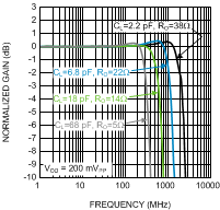 Figure 28. Frequency Response vs Capacitive Load
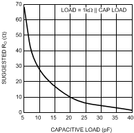 Figure 29. Suggested ROUT vs Capacitive Load
9.2.2 Fully Differential Operation
The LMH6554 will perform best in a fully differential configuration. The circuit shown in Figure 30 is a typical fully differential application circuit as might be used to drive an analog to digital converter (ADC). In this circuit the closed loop gain is AV= VOUT / VIN = RF / RG, where the feedback is symmetric. The series output resistors, RO, are optional and help keep the amplifier stable when presented with a capacitive load. Refer to the Driving Capacitive Loads section for details.
Here is the expression for the input impedance, RIN, as defined in Figure 30:
RIN = 2RG
When driven from a differential source, the LMH6554 provides low distortion, excellent balance, and common mode rejection. This is true provided the resistors RF, RG and RO are well matched and strict symmetry is observed in board layout. With an intrinsic device CMRR of greater than 70 dB, using 0.1% resistors will give a worst case CMRR of around 50 dB for most circuits.
The circuit configuration shown in Figure 30 was used to measure differential S-parameters in a 100Ω environment at a gain of 1 V/V. Refer to Figure 24 in Typical Performance Characteristics VS = ±2.5 V for measurement results.
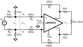 Figure 30. Differential S-Parameter Test Circuit
9.2.3 Single Supply Operation
Single 5V supply operation is possible: however, as discussed earlier, AC input coupling is recommended due to input common mode limitations. An example of an AC coupled, single supply, single-to-differential circuit is shown in Figure 31. Note that when AC coupling, both inputs need to be AC coupled irrespective of single-to-differential or differential-differential configuration. For higher supply voltages DC coupling of the inputs may be possible provided that the output common mode DC level is set high enough so that the amplifier's inputs and outputs are within their specified operation ranges.
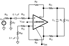 Figure 31. AC Coupled for Single Supply Operation
For optimum performance, split supply operation is recommended using +2.5-V and −2.5-V supplies; however, operation is possible on split supplies as low as +2.35 V and −2.35 V and as high as +2.65 V and −2.65 V. Provided the total supply voltage does not exceed the 4.7-V to 5.3-V operating specification, non-symmetric supply operation is also possible and in some cases advantageous. For example, if a 5-V DC coupled operation is required for low power dissipation but the amplifier input common mode range prevents this operation, it is still possible with split supplies of (V+) and (V-). Where (V+)-(V-) = 5 V and V+ and V- are selected to center the amplifier input common mode range to suit the application.
9.2.4 Driving Analog-to-Digital Converters
Analog-to-digital converters present challenging load conditions. They typically have high impedance inputs with large and often variable capacitive components. Figure 32 shows the LMH6554 driving an ultra-high-speed Gigasample ADC the ADC10D1500. The LMH6554 common mode voltage is set by the ADC10D1500. The circuit in Figure 32 has a 2nd order bandpass LC filter across the differential inputs of the ADC10D1500. The ADC10D1500 is a dual channel 10–bit ADC with maximum sampling rate of 3 GSPS when operating in a single channel mode and 1.5 GSPS in dual channel mode.
Figure 32. Driving a 10-bit Gigasample ADC
Figure 33 shows the SFDR and SNR performance vs. frequency for the LMH6554 and ADC10D1500 combination circuit with the ADC input signal level at −1dBFS. In order to properly match the input impedance seen at the LMH6554 amplifier inputs, RM is chosen to match ZS || RT for proper input balance. The amplifier is configured to provide a gain of 2 V/V in single to differential mode. An external bandpass filter is inserted in series between the input signal source and the amplifier to reduce harmonics and noise from the signal generator.
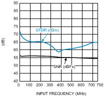 Figure 33. LMH6554 / ADC10D1500 SFDR and SNR Performance vs. Frequency
The amplifier and ADC should be located as close together as possible. Both devices require that the filter components be in close proximity to them. The amplifier needs to have minimal parasitic loading on it's outputs and the ADC is sensitive to high frequency noise that may couple in on its inputs. Some high performance ADCs have an input stage that has a bandwidth of several times its sample rate. The sampling process results in all input signals presented to the input stage mixing down into the first Nyquist zone (DC to Fs/2).
9.2.5 Output Noise Performance and Measurement
Unlike differential amplifiers based on voltage feedback architectures, noise sources internal to the LMH6554 refer to the inputs largely as current sources, hence the low input referred voltage noise and relatively higher input referred current noise. The output noise is therefore more strongly coupled to the value of the feedback resistor and not to the closed loop gain, as would be the case with a voltage feedback differential amplifier. This allows operation of the LMH6554 at much higher gain without incurring a substantial noise performance penalty, simply by choosing a suitable feedback resistor.
Figure 34 shows a circuit configuration used to measure noise figure for the LMH6554 in a 50-Ω system. A feedback resistor value of 200Ω is chosen for the UQFN package to minimize output noise while simultaneously allowing both high gain (7 V/V) and proper 50-Ω input termination. Refer to Single-Ended Input to Differential Output Operation for the calculation of resistor and gain values.
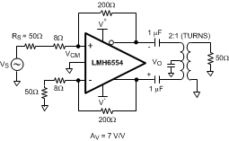 Figure 34. Noise Figure Circuit Configuration
9.2.6 Balanced Cable Driver
With up to 5.68 VPP differential output voltage swing the LMH6554 can be configured as a cable driver. The LMH6554 is also suitable for driving differential cables from a single ended source as shown in Figure 35.
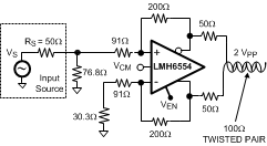 Figure 35. Fully Differential Cable Driver