SNOSB30P October 2008 – January 2015 LMH6554
PRODUCTION DATA.
- 1 Features
- 2 Applications
- 3 Description
- 4 Typical Application Schematic
- 5 Revision History
- 6 Pin Configuration and Functions
- 7 Specifications
- 8 Detailed Description
- 9 Application and Implementation
- 10Power Supply Recommendations
- 11Layout
- 12Device and Documentation Support
- 13Mechanical, Packaging, and Orderable Information
8 Detailed Description
8.1 Overview
The LMH6554 is a fully differential, current feedback amplifier with integrated output common mode control, designed to provide low distortion amplification to wide bandwidth differential signals. The common mode feedback circuit sets the output common mode voltage independent of the input common mode, as well as forcing the V+ and V− outputs to be equal in magnitude and opposite in phase, even when only one of the inputs is driven as in single to differential conversion.
The proprietary current feedback architecture of the LMH6554 offers gain and bandwidth independence with exceptional gain flatness and noise performance, even at high values of gain, simply with the appropriate choice of RF1 and RF2. Generally RF1 is set equal to RF2, and RG1 equal to RG2, so that the gain is set by the ratio RF/RG. Matching of these resistors greatly affects CMRR, DC offset error, and output balance.
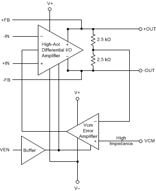
8.2 Functional Block Diagram
8.3 Feature Description
The proprietary current feedback architecture of the LMH6554 offers gain and bandwidth independence with exceptional gain flatness and noise performance, even at high values of gain, simply with the appropriate choice of RF1 and RF2. Generally RF1 is set equal to RF2, and RG1 equal to RG2, so that the gain is set by the ratio RF/RG. Matching of these resistors greatly affects CMRR, DC offset error, and output balance. A maximum of 0.1% tolerance resistors are recommended for optimal performance, and the amplifier is internally compensated to operate with optimum gain flatness with RF value of 200 Ω depending on PCB layout, and load resistance. The output common mode voltage is set by the VCM pin with a fixed gain of 1 V/V. This pin should be driven by a low impedance reference and should be bypassed to ground with a 0.1-μF ceramic capacitor. Any unwanted signal coupling into the VCM pin will be passed along to the outputs, reducing the performance of the amplifier. The LMH6554 can be configured to operate on a single 5V supply connected to V+ with V- grounded or configured for a split supply operation with V+ = +2.5 V and V− = −2.5 V. Operation on a single 5-V supply, depending on gain, is limited by the input common mode range; therefore, AC coupling may be required.
8.4 Device Functional Modes
This wideband FDA requires external resistors for correct signal-path operation. When configured for the desired input impedance and gain setting with these external resistors, the amplifier can be either on with the PD pin asserted to a voltage greater than Vs– + 1.7 V, or turned off by asserting PD low. Disabling the amplifier shuts off the quiescent current and stops correct amplifier operation. The signal path is still present for the source signal through the external resistors. The Vocm control pin sets the output average voltage. Left open, Vocm defaults to an internal midsupply value. Driving this high-impedance input with a voltage reference within its valid range sets a target for the internal Vcm error amplifier.