ZHCSCW7D October   2014  – February 2018 LMH5401

PRODUCTION DATA.  

  1. 特性
  2. 应用
    1.     失真与频率间的关系(G = 12dB,SE-DE,RL = 200Ω,VPP = 2V)
  3. 说明
    1.     驱动 ADC12J4000 的 LMH5401
  4. 修订历史记录
  5. Pin Configuration and Functions
    1.     Pin Functions
  6. Specifications
    1. 6.1 Absolute Maximum Ratings
    2. 6.2 ESD Ratings
    3. 6.3 Recommended Operating Conditions
    4. 6.4 Thermal Information
    5. 6.5 Electrical Characteristics: VS = 5 V
    6. 6.6 Electrical Characteristics: VS = 3.3 V
    7. 6.7 Typical Characteristics: 5 V
    8. 6.8 Typical Characteristics: 3.3 V
    9. 6.9 Typical Characteristics: 3.3-V to 5-V Supply Range
  7. Parameter Measurement Information
    1. 7.1  Output Reference Points
    2. 7.2  ATE Testing and DC Measurements
    3. 7.3  Frequency Response
    4. 7.4  S-Parameters
    5. 7.5  Frequency Response with Capacitive Load
    6. 7.6  Distortion
    7. 7.7  Noise Figure
    8. 7.8  Pulse Response, Slew Rate, and Overdrive Recovery
    9. 7.9  Power Down
    10. 7.10 VCM Frequency Response
    11. 7.11 Test Schematics
  8. Detailed Description
    1. 8.1 Overview
    2. 8.2 Functional Block Diagram
    3. 8.3 Feature Description
      1. 8.3.1 Fully-Differential Amplifier
        1. 8.3.1.1 Power Down and Ground Pins
      2. 8.3.2 Operations for Single-Ended to Differential Signals
        1. 8.3.2.1 AC-Coupled Signal Path Considerations for Single-Ended Input to Differential Output Conversion
        2. 8.3.2.2 DC-Coupled Input Signal Path Considerations for SE-DE Conversions
        3. 8.3.2.3 Resistor Design Equations for Single-to-Differential Applications
        4. 8.3.2.4 Input Impedance Calculations
      3. 8.3.3 Differential-to-Differential Signals
        1. 8.3.3.1 AC-Coupled, Differential-Input to Differential-Output Design Issues
        2. 8.3.3.2 DC-Coupled, Differential-Input to Differential-Output Design Issues
      4. 8.3.4 Output Common-Mode Voltage
      5. 8.3.5 LMH5401 Comparison
    4. 8.4 Device Functional Modes
      1. 8.4.1 Operation With a Split Supply
      2. 8.4.2 Operation With a Single Supply
  9. Application and Implementation
    1. 9.1 Application Information
      1. 9.1.1 Stability
      2. 9.1.2 Input and Output Headroom Considerations
      3. 9.1.3 Noise Analysis
      4. 9.1.4 Noise Figure
      5. 9.1.5 Thermal Considerations
    2. 9.2 Typical Application
      1. 9.2.1 Design Requirements
      2. 9.2.2 Detailed Design Procedure
        1. 9.2.2.1 Driving Matched Loads
        2. 9.2.2.2 Driving Unmatched Loads For Lower Loss
        3. 9.2.2.3 Driving Capacitive Loads
        4. 9.2.2.4 Driving ADCs
          1. 9.2.2.4.1 SNR Considerations
          2. 9.2.2.4.2 SFDR Considerations
          3. 9.2.2.4.3 ADC Input Common-Mode Voltage Considerations : AC-Coupled Input
          4. 9.2.2.4.4 ADC Input Common-Mode Voltage Considerations : DC-Coupled Input
        5. 9.2.2.5 GSPS ADC Driver
        6. 9.2.2.6 Common-Mode Voltage Correction
        7. 9.2.2.7 Active Balun
      3. 9.2.3 Application Curves
    3. 9.3 Do's and Don'ts
      1. 9.3.1 Do:
      2. 9.3.2 Don't:
  10. 10Power Supply Recommendations
    1. 10.1 Supply Voltage
    2. 10.2 Single-Supply
    3. 10.3 Split-Supply
    4. 10.4 Supply Decoupling
  11. 11Layout
    1. 11.1 Layout Guidelines
    2. 11.2 Layout Example
  12. 12器件和文档支持
    1. 12.1 器件支持
      1. 12.1.1 器件命名规则
    2. 12.2 文档支持
      1. 12.2.1 相关文档
    3. 12.3 接收文档更新通知
    4. 12.4 社区资源
    5. 12.5 商标
    6. 12.6 静电放电警告
    7. 12.7 Glossary
  13. 13机械、封装和可订购信息

封装选项

机械数据 (封装 | 引脚)
散热焊盘机械数据 (封装 | 引脚)
订购信息

Stability

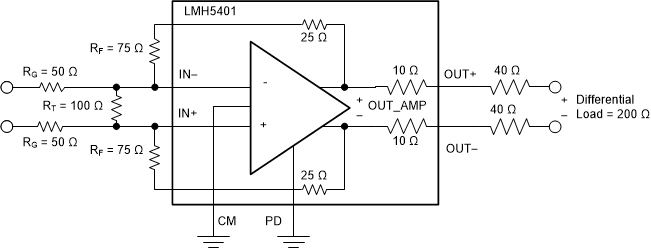
Two types of gain are associated with amplifiers: noise and signal gain. Noise gain (NG) is what is used to best determine the stability of an amplifier. The noise gain is the inverse of the voltage divider from the outputs back to the differential inputs. This gain is calculated by NG = (RF / RIN) + 1. For the LMH5401, NG values greater than three creates a stable circuit independent on how the signal gain is set. In Figure 63, for optimal performance choose RF within the values noted in this document (see the section for further information). Using too large of a resistance in the feedback path adds noise and can possibly have a negative affect on bandwidth, depending on the parasitic capacitance of the board; too low of a resistance can load the output, thus affecting distortion performance. When low gain stability is required, alter the noise gain by adding a dummy resistor (that is, RT in the differential configuration of Figure 63). By manipulating the noise gain with this addition, the amplifier can be stabilized without affecting signal gain. Evaluate the system at lower signal gains (G less than or equal to 2) if SNR can be tolerated with the higher noise gain configuration. In Figure 63, RS and RT in parallel combination affects the noise gain of the amplifier. RG and RF are the main gain-setting resistors and the addition of RT adjusts the noise gain for stability. Much of this stability can be simulated using the LMH5401 TINA model, depending on the amplifier configuration. The example in Figure 63 ( listed in row 1 of Table 1) uses the LMH5401, a signal gain of two , and a noise gain of five.
LMH5401 ai_stability_sbos710.gifFigure 63. Differential Stability