ZHCSCW7D October   2014  – February 2018 LMH5401

PRODUCTION DATA.  

  1. 特性
  2. 应用
    1.     失真与频率间的关系(G = 12dB,SE-DE,RL = 200Ω,VPP = 2V)
  3. 说明
    1.     驱动 ADC12J4000 的 LMH5401
  4. 修订历史记录
  5. Pin Configuration and Functions
    1.     Pin Functions
  6. Specifications
    1. 6.1 Absolute Maximum Ratings
    2. 6.2 ESD Ratings
    3. 6.3 Recommended Operating Conditions
    4. 6.4 Thermal Information
    5. 6.5 Electrical Characteristics: VS = 5 V
    6. 6.6 Electrical Characteristics: VS = 3.3 V
    7. 6.7 Typical Characteristics: 5 V
    8. 6.8 Typical Characteristics: 3.3 V
    9. 6.9 Typical Characteristics: 3.3-V to 5-V Supply Range
  7. Parameter Measurement Information
    1. 7.1  Output Reference Points
    2. 7.2  ATE Testing and DC Measurements
    3. 7.3  Frequency Response
    4. 7.4  S-Parameters
    5. 7.5  Frequency Response with Capacitive Load
    6. 7.6  Distortion
    7. 7.7  Noise Figure
    8. 7.8  Pulse Response, Slew Rate, and Overdrive Recovery
    9. 7.9  Power Down
    10. 7.10 VCM Frequency Response
    11. 7.11 Test Schematics
  8. Detailed Description
    1. 8.1 Overview
    2. 8.2 Functional Block Diagram
    3. 8.3 Feature Description
      1. 8.3.1 Fully-Differential Amplifier
        1. 8.3.1.1 Power Down and Ground Pins
      2. 8.3.2 Operations for Single-Ended to Differential Signals
        1. 8.3.2.1 AC-Coupled Signal Path Considerations for Single-Ended Input to Differential Output Conversion
        2. 8.3.2.2 DC-Coupled Input Signal Path Considerations for SE-DE Conversions
        3. 8.3.2.3 Resistor Design Equations for Single-to-Differential Applications
        4. 8.3.2.4 Input Impedance Calculations
      3. 8.3.3 Differential-to-Differential Signals
        1. 8.3.3.1 AC-Coupled, Differential-Input to Differential-Output Design Issues
        2. 8.3.3.2 DC-Coupled, Differential-Input to Differential-Output Design Issues
      4. 8.3.4 Output Common-Mode Voltage
      5. 8.3.5 LMH5401 Comparison
    4. 8.4 Device Functional Modes
      1. 8.4.1 Operation With a Split Supply
      2. 8.4.2 Operation With a Single Supply
  9. Application and Implementation
    1. 9.1 Application Information
      1. 9.1.1 Stability
      2. 9.1.2 Input and Output Headroom Considerations
      3. 9.1.3 Noise Analysis
      4. 9.1.4 Noise Figure
      5. 9.1.5 Thermal Considerations
    2. 9.2 Typical Application
      1. 9.2.1 Design Requirements
      2. 9.2.2 Detailed Design Procedure
        1. 9.2.2.1 Driving Matched Loads
        2. 9.2.2.2 Driving Unmatched Loads For Lower Loss
        3. 9.2.2.3 Driving Capacitive Loads
        4. 9.2.2.4 Driving ADCs
          1. 9.2.2.4.1 SNR Considerations
          2. 9.2.2.4.2 SFDR Considerations
          3. 9.2.2.4.3 ADC Input Common-Mode Voltage Considerations : AC-Coupled Input
          4. 9.2.2.4.4 ADC Input Common-Mode Voltage Considerations : DC-Coupled Input
        5. 9.2.2.5 GSPS ADC Driver
        6. 9.2.2.6 Common-Mode Voltage Correction
        7. 9.2.2.7 Active Balun
      3. 9.2.3 Application Curves
    3. 9.3 Do's and Don'ts
      1. 9.3.1 Do:
      2. 9.3.2 Don't:
  10. 10Power Supply Recommendations
    1. 10.1 Supply Voltage
    2. 10.2 Single-Supply
    3. 10.3 Split-Supply
    4. 10.4 Supply Decoupling
  11. 11Layout
    1. 11.1 Layout Guidelines
    2. 11.2 Layout Example
  12. 12器件和文档支持
    1. 12.1 器件支持
      1. 12.1.1 器件命名规则
    2. 12.2 文档支持
      1. 12.2.1 相关文档
    3. 12.3 接收文档更新通知
    4. 12.4 社区资源
    5. 12.5 商标
    6. 12.6 静电放电警告
    7. 12.7 Glossary
  13. 13机械、封装和可订购信息

封装选项

机械数据 (封装 | 引脚)
散热焊盘机械数据 (封装 | 引脚)
订购信息

Typical Characteristics: 3.3 V

at TA = 25°C, split supplies, VCM = 0 V, RL = 200-Ω differential (RO = 40 Ω each), G = 12 dB, single-ended input and differential output, and input and output pins referenced to midsupply, (unless otherwise noted). Measured using an EVM as discussed in the section (see Figure 56 to Figure 59).
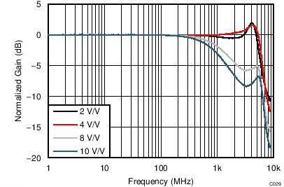
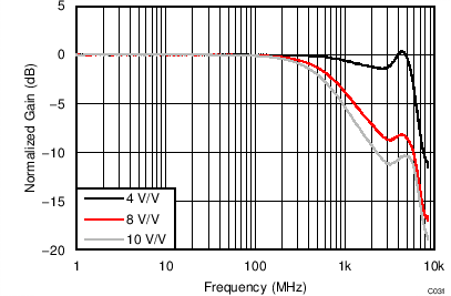
LMH5401 TC_C029_Freq_Gain_3p3V_0p2Vpp.png
VS = ±1.65 V, VOUT_AMP = 0.2 VPP, RL = 200 Ω
Figure 29. Small-Signal Frequency Response vs Gain
LMH5401 TC_C031_Freq_RLd_3p3V_0p2vpp.png
VS = ±1.65 V, VOUT_AMP = 0.2 VPP, G = 12 dB
Figure 31. Small-Signal Frequency Response vs RL
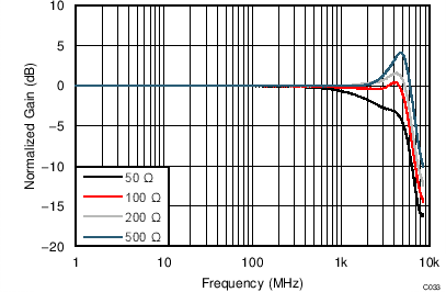
LMH5401 TC_C033_Freq_RLoad_3p3V_0p2Vpp.png
VS = ±1.65 V, VOUT_AMP = 0.2 VPP, G = 12 dB
Figure 33. Small-Signal Differential Input Frequency Response vs RL
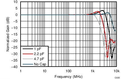
LMH5401 TC_C035_Freq_CLoad_3p3V_0p2Vpp.png
VS = ±1.65 V, VOUT_AMP = 2 VPP, capacitance at DUT output pins,
Figure 35. Small-Signal Frequency Response with Capacitive Load
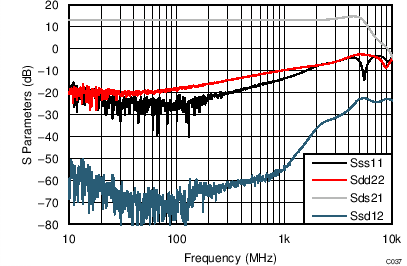
LMH5401 TC_C037_Sparam_SEin_3V.png
VS = ±1.65 V, VOUT_AMP = 200 mVPP
Figure 37. Single-Ended Input, S-Parameters
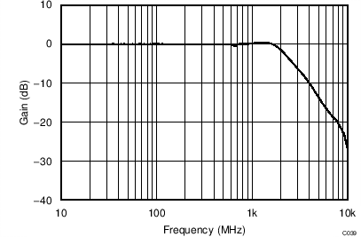
LMH5401 TC_C039_Freq_CM_0p2Vpp_3p3V.png
VS = ±1.65 V, VOUT_AMP = 200 mVPP
Figure 39. Common-Mode Frequency Response
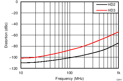
LMH5401 TC_C041_H23_3V_Freq_DiffIn.png
VS = ±1.65 V, VOUT_AMP = 1 VPP, RL = 200 Ω, G = 12 dB, differential input
Figure 41. HD2 and HD3 Differential
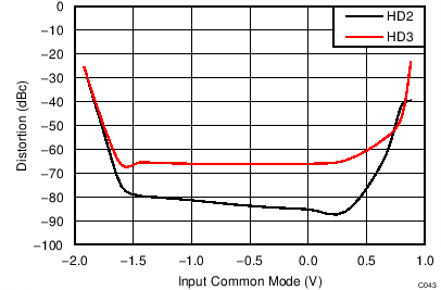
LMH5401 TC_C043_H23_3V_Vicm.png
VS = ±1.65 V, VOUT_AMP = 1 VPP, f = 500 MHz, RL = 200 Ω, G = 12 dB
Figure 43. HD2 and HD3 vs Input Common-Mode Voltage
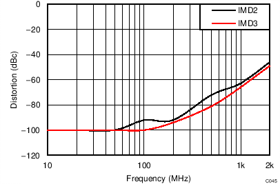
LMH5401 TC_C045_IMD23_Frequency_3p3V.png
VS = ±1.65 V, VOUT_AMP = 0.5 VPP per tone, RL = 200 Ω, G = 12 dB
Figure 45. Intermodulation Distortion vs Frequency
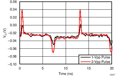
LMH5401 TC_C047_Pulse_3p3V_CM.png
VS = ±1.65 V, VOUT_AMP, VCM = (VO+ + VO–) / 2
Figure 47. Pulse Response Common-Mode
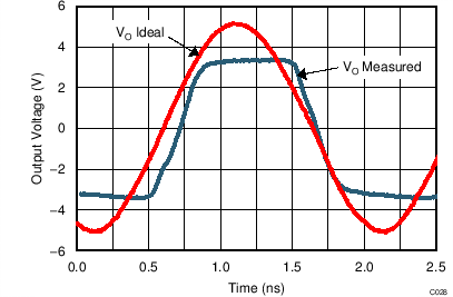
LMH5401 TC_C028_Overdrive_5v_bos695.png
VS = ±2.5 V
Figure 49. Overdrive Recovery
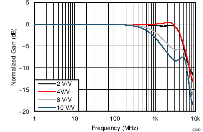
LMH5401 TC_C030_Freq_Gain_3p3V_2Vpp.png
VS = ±1.65 V, VOUT_AMP = 2 VPP, RL = 200 Ω
Figure 30. Large-Signal Frequency Response vs Gain
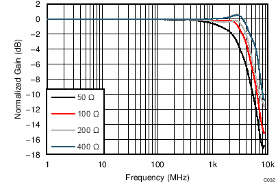
LMH5401 TC_C032_Freq_RLoad_3p3V_2Vpp.png
VS = ±1.65 V, VOUT_AMP = 2 VPP, G = 12 dB
Figure 32. Large-Signal Frequency Response vs RL
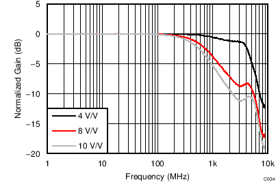
LMH5401 TC_C034_Freq_RL_3p3V_2Vpp_dif.png
VS = ±1.65 V, VOUT_AMP = 2 VPP
Figure 34. Large-Signal Differential Input Frequency Response vs RL
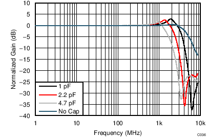
LMH5401 TC_C036_Freq_CLoad_3p3V_2Vpp.png
VS = ±1.65 V, VOUT_AMP = 2 VPP, capacitance at DUT output pins
Figure 36. Large-Signal Frequency Response with Capacitive Load
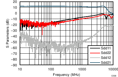
LMH5401 TC_C038_Sparam_3V_Diff.png
VS = ±1.65 V, VOUT_AMP = 200 mVPP
Figure 38. Differential Input, S-Parameters
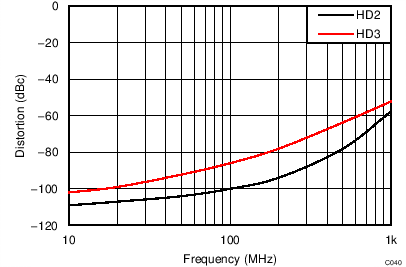
LMH5401 TC_C040_H23_3V_Freq_SEIn.png
VS = ±1.65 V, VOUT_AMP = 1 VPP, RL = 200 Ω, G = 12 dB, single-ended input
Figure 40. HD2 and HD3
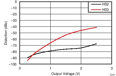
LMH5401 TC_C042_H23_3V_Vout.png
VS = ±1.65, VOUT_AMP = 1 VPP, f = 500 MHz, RL = 200 Ω, G = 12 dB
Figure 42. HD2 and HD3 vs Output Voltage
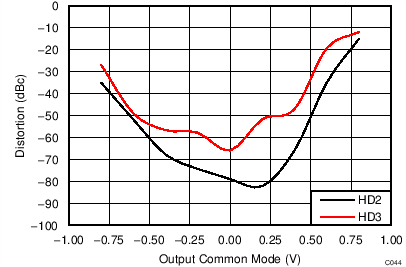
LMH5401 TC_C044_H23_3V_Vocm.png
VS = ±1.65 V, VOUT_AMP = 1 VPP, f = 500 MHz, RL = 200 Ω, G = 12 dB
Figure 44. HD2 and HD3 vs Output Common-Mode Voltage
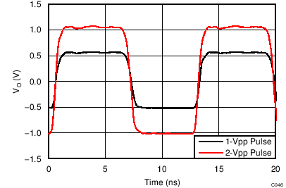
LMH5401 TC_C046_Pulse_3p3V_Diff.png
VS = ±1.65 V, VOUT_AMP
Figure 46. Pulse Response for Various VO
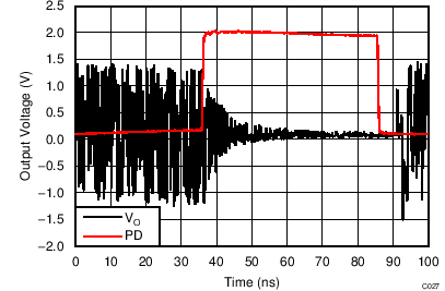
LMH5401 TC_C027_PDTime_5V_bos695.png
VS = ±2.5 V
Figure 48. Power-Down Timing