ZHCSH86B December   2017  – February 2019 LMH5401-SP

PRODUCTION DATA.  

  1. 特性
  2. 应用
  3. 说明
    1.     Device Images
      1.      LMH5401-SP 小信号频率响应
      2.      LMH5401-SP 驱动 ADC12D1620QML
  4. 修订历史记录
  5. 说明 (续)
  6. Pin Configuration and Functions
    1.     Pin Functions
  7. Specifications
    1. 7.1 Absolute Maximum Ratings
    2. 7.2 ESD Ratings
    3. 7.3 Recommended Operating Conditions
    4. 7.4 Thermal Information
    5. 7.5 Electrical Characteristics: VS = 5 V
    6. 7.6 Electrical Characteristics: VS = 3.3 V
    7. 7.7 Typical Characteristics: 5 V
    8. 7.8 Typical Characteristics: 3.3 V
  8. Parameter Measurement Information
    1. 8.1  Output Reference Nodes and Gain Nomenclature
    2. 8.2  ATE Testing and DC Measurements
    3. 8.3  Frequency Response
    4. 8.4  S-Parameters
    5. 8.5  Frequency Response with Capacitive Load
    6. 8.6  Distortion
    7. 8.7  Noise Figure
    8. 8.8  Pulse Response, Slew Rate, and Overdrive Recovery
    9. 8.9  Power Down
    10. 8.10 VCM Frequency Response
    11. 8.11 Test Schematics
  9. Detailed Description
    1. 9.1 Overview
    2. 9.2 Functional Block Diagram
    3. 9.3 Feature Description
      1. 9.3.1 Fully-Differential Amplifier
      2. 9.3.2 Operations for Single-Ended to Differential Signals
        1. 9.3.2.1 AC-Coupled Signal Path Considerations for Single-Ended Input to Differential Output Conversion
        2. 9.3.2.2 DC-Coupled Input Signal Path Considerations for SE-DE Conversions
        3. 9.3.2.3 Resistor Design Equations for Single-to-Differential Applications
        4. 9.3.2.4 Input Impedance Calculations
      3. 9.3.3 Differential-to-Differential Signals
        1. 9.3.3.1 AC-Coupled, Differential-Input to Differential-Output Design Issues
        2. 9.3.3.2 DC-Coupled, Differential-Input to Differential-Output Design Issues
      4. 9.3.4 Output Common-Mode Voltage
    4. 9.4 Device Functional Modes
      1. 9.4.1 Operation With a Split Supply
      2. 9.4.2 Operation With a Single Supply
  10. 10Application and Implementation
    1. 10.1 Application Information
      1. 10.1.1 Stability, Noise Gain, and Signal Gain
      2. 10.1.2 Input and Output Headroom Considerations
      3. 10.1.3 Noise Analysis
      4. 10.1.4 Noise Figure
      5. 10.1.5 Thermal Considerations
    2. 10.2 Typical Application
      1. 10.2.1 Design Requirements
      2. 10.2.2 Detailed Design Procedure
        1. 10.2.2.1 Driving Matched Loads
        2. 10.2.2.2 Driving Unmatched Loads For Lower Loss
        3. 10.2.2.3 Driving Capacitive Loads
        4. 10.2.2.4 Driving ADCs
          1. 10.2.2.4.1 SNR Considerations
          2. 10.2.2.4.2 SFDR Considerations
          3. 10.2.2.4.3 ADC Input Common-Mode Voltage Considerations—AC-Coupled Input
          4. 10.2.2.4.4 ADC Input Common-Mode Voltage Considerations—DC-Coupled Input
        5. 10.2.2.5 GSPS ADC Driver
        6. 10.2.2.6 Common-Mode Voltage Correction
        7. 10.2.2.7 Active Balun
      3. 10.2.3 Application Curves
    3. 10.3 Do's and Don'ts
      1. 10.3.1 Do:
      2. 10.3.2 Don't:
  11. 11Power Supply Recommendations
    1. 11.1 Supply Voltage
    2. 11.2 Single Supply
    3. 11.3 Split Supply
    4. 11.4 Supply Decoupling
  12. 12Layout
    1. 12.1 Layout Guidelines
    2. 12.2 Layout Example
  13. 13器件和文档支持
    1. 13.1 器件支持
      1. 13.1.1 器件命名规则
    2. 13.2 文档支持
      1. 13.2.1 相关文档
    3. 13.3 接收文档更新通知
    4. 13.4 社区资源
    5. 13.5 商标
    6. 13.6 静电放电警告
    7. 13.7 术语表
  14. 14机械、封装和可订购信息

封装选项

机械数据 (封装 | 引脚)
散热焊盘机械数据 (封装 | 引脚)
订购信息

AC-Coupled, Differential-Input to Differential-Output Design Issues

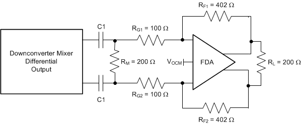
When using the LMH5401-SP with an ac-coupled differential source, the input can be coupled in through two blocking capacitors. An optional input differential termination resistor (RM) can be included to allow the input RG resistors to be scaled up while still delivering lower differential input impedance to the source. In Figure 60, the RG elements sum to show a 200-Ω differential impedance and the RM element combines in parallel to give a net 100-Ω, ac, differential impedance to the source. Again, the design proceeds ideally by selecting the RF element values, then the RG to set the differential gain, then an RM element (if needed) to achieve a target input impedance. Alternatively, the RM element can be eliminated, the RG elements set to the desired input impedance, and RF set to the get the differential gain (= RF / RG). The dc biasing in Figure 60 is very simple. The output VOCM is set by the input control voltage and, because there is no dc current path for the output common-mode voltage, that dc bias also sets the input pins common-mode operating points.
LMH5401-SP ai_downconvert_mixer_bos710.gifFigure 60. Downconverting Mixer AC-Coupled to the LMH5401-SP (GV = 4 V/V)