ZHCSKC6D October 2019 – January 2023 LMH32401
PRODUCTION DATA
- 1 特性
- 2 应用
- 3 说明
- 4 Revision History
- 5 Pin Configuration and Functions
-
6 Specifications
- 6.1 Absolute Maximum Ratings
- 6.2 ESD Ratings
- 6.3 Recommended Operating Conditions
- 6.4 Thermal Information
- 6.5 Electrical Characteristics: Gain = 2 kΩ
- 6.6 Electrical Characteristics: Gain = 20 kΩ
- 6.7 Electrical Characteristics: Both Gains
- 6.8 Electrical Characteristics: Logic Threshold and Switching Characteristics
- 6.9 Typical Characteristics
- 7 Detailed Description
- 8 Application and Implementation
- 9 Power Supply Recommendations
- 10Layout
- 11Device and Documentation Support
- 12Mechanical, Packaging, and Orderable Information
封装选项
请参考 PDF 数据表获取器件具体的封装图。
机械数据 (封装 | 引脚)
- RGT|16
- Y|0
散热焊盘机械数据 (封装 | 引脚)
- RGT|16
订购信息
5 Pin Configuration and Functions
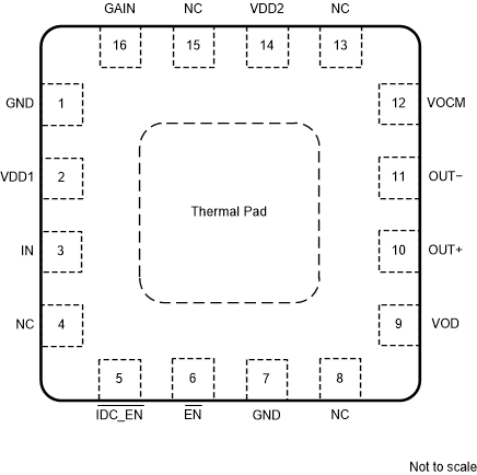
 Figure 5-1 RGT Package, 16-Pin VQFN with
Exposed Thermal Pad (Top View)
 Table 5-1 Pin Functions
| PIN | TYPE(2) | DESCRIPTION | |
|---|---|---|---|
| NAME | NO. | ||
| EN | 6 | I | Device enable pin. EN = logic low = normal operation (default)(1); EN = logic high = power off mode. |
| GAIN | 16 | I | Gain setting. GAIN = low = 2 kΩ (default)(1); GAIN = high = 20 kΩ. |
| GND | 1, 7 | I | Amplifier ground. |
| IDC_EN | 5 | I | Ambient light cancellation (ALC) loop enable. IDC_EN = logic low = enable DC current cancellation (default)(1); IDC_EN = logc high = disable DC current cancellation. |
| IN | 3 | I | Transimpedance amplifier input. |
| NC | 4, 8, 13, 15 | — | No connection. |
| OUT– | 11 | O | Inverting amplifier output. When light is incident on the photodiode the output pin transitions in a negative direction from the no light condition (APD anode connected to negative bias). |
| OUT+ | 10 | O | Noninverting amplifier output. When light is incident on the photodiode the output pin transitions in a positive direction from the no light condition (APD anode connected to negative bias). |
| VDD1 | 2 | I | Positive power supply for the transimpedance amplifier stage. |
| VDD2 | 14 | I | Positive power supply for the differential amplifier stage. Tie VDD1 and VDD2 to the same power supply with independent power-supply bypassing. |
| VOCM | 12 | I | Differential amplifier common-mode output setting. |
| VOD | 9 | I | Differential amplifier differential output offset setting. |
| Thermal pad | — | Connect the thermal pad to GND or the most negative power supply of the device under test (DUT). | |
(1) TI recommends driving a digital pin with a low-impedance source rather than leaving the pin floating because fast-moving transients can couple into the pin and inadvertently change the logic level.
(2) I = input, O = output
| DIE THICKNESS | BACKSIDE FINISH | BACKSIDE POTENTIAL | BOND PAD METALLIZATION |
|---|---|---|---|
| 381 μm | Silicon with backgrind | Wafer backside is not electrically isolated and should be held at the same potential as the most negative power supply connected to the die (GND) | AlCu |
Figure 5-2 Bare Die Package
Table 5-2 Bond Pad Coordinates of Bare Die Version in Microns
| PAD NUMBER | PAD NAME | X-MIN | Y-MIN | X-MAX | Y-MAX |
|---|---|---|---|---|---|
| 1 | GND | 15 | 711.4 | 90 | 786.4 |
| 2 | VDD1 | 15 | 543 | 90 | 618 |
| 3 | IN | 15 | 362 | 90 | 437 |
| 4 | NC | 15 | 201 | 90 | 276 |
| 5 | IDC_EN | 124.675 | 15 | 199.675 | 90 |
| 6 | EN | 286.675 | 15 | 361.675 | 90 |
| 7 | GND | 547.7 | 15 | 622.7 | 90 |
| 8 | NC | 713.675 | 15 | 788.675 | 90 |
| 9 | VOD | 855 | 169.075 | 930 | 244.075 |
| 10 | OUT+ | 855 | 307.6 | 930 | 382.6 |
| 11 | NC | 855 | 452.5 | 930 | 527.5 |
| 12 | OUT- | 855 | 597.325 | 930 | 672.325 |
| 13 | VOCM | 855 | 736.05 | 930 | 811.05 |
| 14 | NC | 713.65 | 890 | 788.65 | 965 |
| 15 | VDD2 | 547.675 | 890 | 622.675 | 965 |
| 16 | NC | 286.675 | 890 | 361.675 | 965 |
| 17 | GAIN | 124.675 | 890 | 199.675 | 965 |