ZHCSIC8B April   2016  – June 2018 LMH0324

PRODUCTION DATA.  

  1. 特性
  2. 应用
  3. 说明
    1.     Device Images
      1.      简化框图
  4. 修订历史记录
  5. Pin Configuration and Functions
    1.     Pin Functions
  6. Specifications
    1. 6.1 Absolute Maximum Ratings
    2. 6.2 ESD Ratings
    3. 6.3 Recommended Operating Conditions
    4. 6.4 Thermal Information
    5. 6.5 Electrical Characteristics
    6. 6.6 Recommended SMBus Interface AC Timing Specifications
    7. 6.7 Serial Parallel Interface (SPI) AC Timing Specifications
    8. 6.8 Typical Characteristics
  7. Detailed Description
    1. 7.1 Overview
    2. 7.2 Functional Block Diagram
    3. 7.3 Feature Description
      1. 7.3.1 4-Level Input Configuration Pins
      2. 7.3.2 Carrier Detect
      3. 7.3.3 Adaptive Cable Equalizer
      4. 7.3.4 Launch Amplitude
      5. 7.3.5 Input-Output Mux Selection
      6. 7.3.6 Output Function Control
      7. 7.3.7 Output Driver Amplitude and De-Emphasis Control
      8. 7.3.8 Additional Programmability
        1. 7.3.8.1 Cable Length Indicator (CLI)
        2. 7.3.8.2 Digital MUTEREF
    4. 7.4 Device Functional Modes
      1. 7.4.1 System Management Bus (SMBus) Mode
        1. 7.4.1.1 SMBus Read and Write Transactions
          1. 7.4.1.1.1 SMBus Write Operation Format
          2. 7.4.1.1.2 SMBus Read Operation Format
      2. 7.4.2 Serial Peripheral Interface (SPI) Mode
        1. 7.4.2.1 SPI Read and Write Transactions
          1. 7.4.2.1.1 SPI Write Transaction Format
          2. 7.4.2.1.2 SPI Read Transaction Format
        2. 7.4.2.2 SPI Daisy Chain
    5. 7.5 LMH0324 Register Map
      1. 7.5.1 Share Register Page
      2. 7.5.2 CableEQ/Drivers Register Page
  8. Application and Implementation
    1. 8.1 Application Information
      1. 8.1.1 General Guidance for SMPTE Applications
    2. 8.2 Typical Application
      1. 8.2.1 Design Requirements
      2. 8.2.2 Detailed Design Procedure
      3. 8.2.3 Recommended VOD and DE Register Settings
      4. 8.2.4 Application Performance Plots
  9. Power Supply Recommendations
  10. 10Layout
    1. 10.1 Layout Guidelines
    2. 10.2 Layout Example
  11. 11器件和文档支持
    1. 11.1 接收文档更新通知
    2. 11.2 社区资源
    3. 11.3 商标
    4. 11.4 静电放电警告
    5. 11.5 术语表
  12. 12机械、封装和可订购信息

封装选项

请参考 PDF 数据表获取器件具体的封装图。

机械数据 (封装 | 引脚)
  • RTW|24
散热焊盘机械数据 (封装 | 引脚)
订购信息

SPI Daisy Chain

The LMH0324 supports SPI daisy-chaining among multiple devices, as shown in Figure 15.
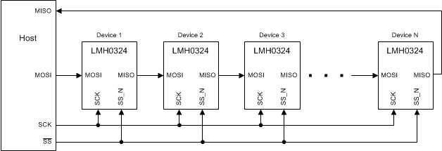
LMH0324 daisy_chain_configuration_snls516.gifFigure 15. Daisy-Chain Configuration

Each LMH0324 device is directly connected to the SCK and SS_N pins of the host. The first LMH0324 device in the chain is connected to the host’s MOSI pin, and the last device in the chain is connected to the host’s MISO pin. The MOSI pin of each intermediate LMH0324 device in the chain is connected to the MISO pin of the previous LMH0324 device, thereby creating a serial shift register. In a daisy-chain configuration of N x LMH0324 devices, the host conceptually sees a shift register of length 17 x N for a basic SPI transaction, during which SS_N is asserted low for 17 x N clock cycles.