SNAS254B October 2006 – April 2017 LM98714
PRODUCTION DATA.
- 1 Features
- 2 Applications
- 3 Description
- 4 Revision History
- 5 Pin Configuration and Functions
- 6 Specifications
-
7 Detailed Description
- 7.1 Overview
- 7.2 Functional Block Diagram
- 7.3
Feature Description
- 7.3.1 Input Clock Introduction
- 7.3.2
Modes of Operation
- 7.3.2.1 Mode 3 - Three Channel Input/Synchronous Pixel Sampling
- 7.3.2.2 Mode 2 - Two Channel Input/Synchronous Pixel Sampling
- 7.3.2.3 Mode 1a - One Channel Input/One, Two, Three, Four, or Five Color Sequential Line Sampling
- 7.3.2.4 Mode 1b - One Channel Input Per Line/Sequential Line (Input) Sampling/Three Channel Processing
- 7.3.3 Input Bias and Clamping
- 7.3.4 Coarse Pixel Phase Alignment
- 7.3.5 Internal Sample Timing
- 7.3.6 Automatic Black Level Correction Loop
- 7.3.7 Internal Timing Generation
- 7.3.8 CCD Timing Generator Master/Slave Modes
- 7.3.9 LVDS Output Mode
- 7.3.10 CMOS Output Mode
- 7.3.11 CMOS Output Data Latency Diagrams
- 7.4
Device Functional Modes
- 7.4.1 Mode 3 - Three Channel Input/Synchronous Pixel Sampling
- 7.4.2 Mode 2 - Two Channel Input/Synchronous Pixel Sampling
- 7.4.3 Mode 1a - One Channel Input/One, Two, Three, Four, Or Five Color Sequential Line Sampling
- 7.4.4 Mode 1b - One Channel Color Input Per Line/Sequential Line (Input) Sampling/Three Channel Processing
- 7.5 Programming
- 7.6 Register Maps
- 8 Application and Implementation
- 9 Device and Documentation Support
- 10Mechanical, Packaging, and Orderable Information
7 Detailed Description
7.1 Overview
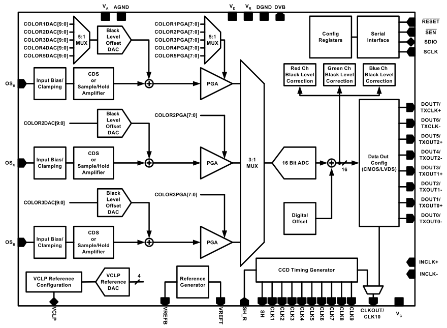
The LM98714 is a 16-bit, three-input, complete Analog Front End (AFE) for digital color copier and Multi-Function Peripheral (MFP) applications. The system block diagram of the LM98714, shown in Functional Block Diagram highlights the main features of the device. Each input has its own Input Bias and Clamping Network which are routed through a selectable Sample/Hold (S/H) or Correlated Double Sampler (CDS) amplifier. A ±9-Bit Offset DAC applies independent offset correction for each channel. A -3 to 17.9dB Programmable Gain Amplifier (PGA) applies independent gain correction for each channel. The LM98714 also provides independent Digital Black Level Correction Feedback Loops for each channel. The Black Level Correction Loop can be configured to run in Manual Mode (where the user inputs their own values of DAC offset) or in Automatic Mode where the LM98714 calculates each channel’s Offset DAC value during optical black pixels and then adjusts the Offset register accordingly. The signals are routed to a single high performance 16-bit, 45 MHz analog-to-digital converter.
7.2 Functional Block Diagram
7.3 Feature Description
7.3.1 Input Clock Introduction
The clock input to the LM98714 can be a differential LVDS clock on the INCLK+ and INCLK- pins or a CMOS level clock applied to the INCLK+ pin with the INCLK- pin connected to DGND. The external clock signal format is auto sensed internally. In addition to the two available level formats, the input clock can be applied at the Pixel frequency (PIXCLK) or at the ADC frequency (ADCCLK). The LM98714 can perform internal clock multiplication when a Pixel frequency clock is applied, or no multiplication when an ADC frequency clock is applied. The internal configuration registers need to be written to perform the proper setup of the input clock. Table 1 shows the available input clock configurations for each operating mode.
Table 1. Input Clock Configurations
| AFE Mode | Input Clock Type | Internal Multiplier |
INCLK Max Freq. |
Configuration Register Settings |
|---|---|---|---|---|
| Mode 3 | INCLK = Pixel Freq. (PIXCLK) | 3x | 15 MHz | PIXCLK Configuration: Main Config Reg 1, Bit[2] = 1'b1 |
| INCLK = ADC Freq. (ADCCLK) | 1x | 45 MHz | ADCCLK Configuration: Main Config Reg 1, Bit[2] = 1'b0 | |
| Mode 2 | INCLK = Pixel Freq. (PIXCLK) | 2x | 22.5 MHz | PIXCLK Configuration: Main Config Reg 1, Bit[2] = 1'b1 |
| INCLK = ADC Freq. (ADCCLK) | 1x | 45 MHz | ADCCLK Configuration: Main Config Reg 1, Bit[2] = 1'b0 | |
| Mode 1 | INCLK = Pixel Freq. = ADC Freq (ADCCLK = PIXCLK in Mode 1) |
1x | 30MHz | Main Config Reg 1, Bit[2] = 1'bx |
7.3.2 Modes of Operation
The LM98714 can be configured to operate in several different operating modes. The following sections are a brief introduction to these modes of operation. A more rigorous explanation of the operating modes is contained in the Modes of Operation section. including input sampling diagrams for each mode as well as a description of the operating conditions.
7.3.2.1 Mode 3 - Three Channel Input/Synchronous Pixel Sampling
OSB, OSG, and OSR inputs are sampled synchronously at a pixel rate. The sampled signals are processed with each channel’s offset and gain adjusted independently via the control registers. The order in which pixels are processed from the input to the ADC is fully programmable and is synchronized by the SH pulse. In this mode, the maximum channel speed is 15MSPS per channel with the ADC running at 45MSPS yielding a three color throughput of 45MSPS.
7.3.2.2 Mode 2 - Two Channel Input/Synchronous Pixel Sampling
Mode 2 is useful for CCD sensors with a Black and White mode with Even and Odd outputs. In its default configuration, Mode 2 samples the Even output via the OSB channel input, and the Odd output via the OSG channel input. Sampling of the Even and Odd pixels is performed synchronously at a maximum sample rate of 22.5MSPS per input with the ADC running at 45MSPS.
7.3.2.3 Mode 1a - One Channel Input/One, Two, Three, Four, or Five Color Sequential Line Sampling
In Mode 1a, all pixels are processed through a single input (OSR, OSG, or OSB) chosen through the control register setup. This mode is useful in applications where only one input channel is used. The selected input is programmable through the control register. If more than one color is being sent to the input, the user can configure the OSR channel to utilize up to five offset and gain coefficients for up to five different lines of color pixels. The SH pulse at the beginning of each line sequences the DAC and PGA coefficients as configured in the control registers. In this mode, the maximum channel speed is 30MSPS per channel with the ADC running at 30MSPS.
7.3.2.4 Mode 1b - One Channel Input Per Line/Sequential Line (Input) Sampling/Three Channel Processing
In Mode 1b the OSR, OSG, and OSB inputs are sampled one input per line with the input selection being sequenced to the next color by an SH pulse. This mode is useful with sensors that output whole lines of pixels of a single color. The order in which the inputs are sampled is fully programmable. Sequencing from one channel to the next is triggered by the SH pulse. The first SH pulse after this mode is set (or reset) sets up the first programmed input for gain and offset and initiates sampling through that input alone. The next SH pulse switches the active input to the second channel indicated by the configuration registers. This sequencing with SH pulses continues to the third input and then continuously loops through the inputs. In this mode, the maximum channel speed is 30MSPS per channel with the ADC running at 30MSPS.
7.3.3 Input Bias and Clamping
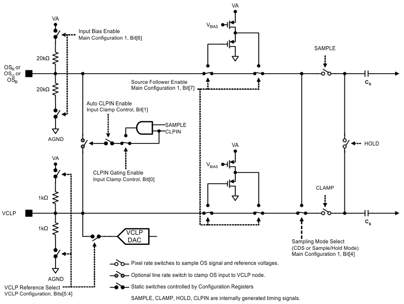 Figure 2. Input Bias and Clamping Diagram
The inputs to the LM98714 are typically AC coupled through a film capacitor and can be sampled in either Sample and Hold Mode (S/H Mode) or Correlated Double Sampling Mode (CDS Mode). In either mode, the DC bias point for the LM98714 side of the AC coupling capacitor is set using the circuit of Figure 2 which can be configured to operate in a variety of different modes.
A typical CCD waveform is shown in Figure 3. Also shown in Figure 3 is an internal signal “SAMPLE” which can be used to “gate” the CLPIN signal so that it only occurs during the “signal” portion of the CCD pixel waveform.
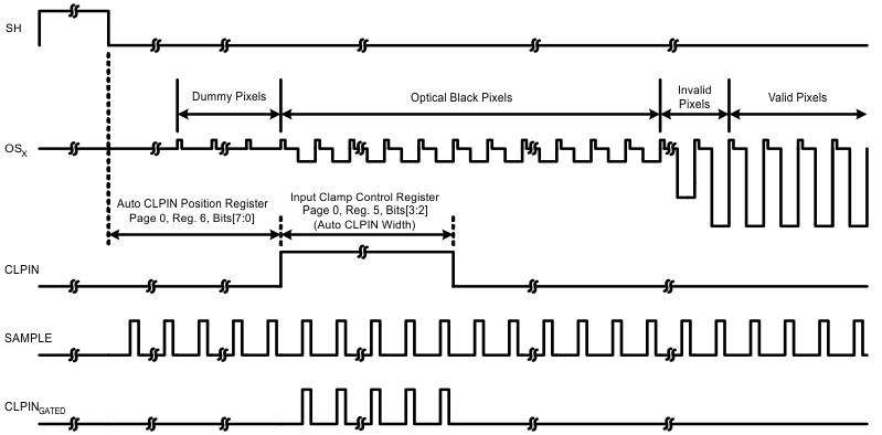 Figure 3. Typical CCD Waveform and LM98714 Input Clamp Signal (CLPIN)
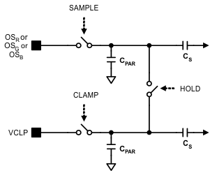 Figure 4. Sample and Hold Mode Simplified Input Diagram
Proper DC biasing of the CCD waveform in Sample and Hold mode is critical for realizing optimal operating conditions. In Sample/Hold mode, the Signal Level of the CCD waveform is compared to the DC voltage on the VCLP pin. In order to fully utilize the range of the input circuitry, it is desirable to cause the Black Level signal voltage to be as close to the VCLP voltage as possible, resulting in a near zero scale output for Black Level pixels.
In Sample/Hold Mode, the DC bias point of the input pin is typically set by actuating the input clamp switch (see Figure 2) during optical black pixels which connects the input pins to the VCLP pin DC voltage. The signal controlling this switch is an auto-generated pulse, CLPIN. CLPIN is generated with a programmable pixel delay with respect to SH and a programmable pixel width. These parameters are available through the serial interface control registers.
Actuating the input clamp will force the average value of the CCD waveform to be centered around the VCLP DC voltage. During Optical Black Pixels, the CCD output has roughly three components. The first component of the pixel is a “Reset Noise” peak followed by the Reset (or Pedestal) Level voltage, then finally the Black Level voltage signal. Taking the average of these signal components will result in a final “clamped” DC bias point that is close to the Black Level signal voltage.
To provide a more precise DC bias point (i.e. a voltage closer to the Black Level voltage), the CLPIN pulse can be “gated” by the internally generated SAMPLE clock. This resulting CLPINGATED signal is the logical “AND” of the SAMPLE and CLPIN signals as shown in Figure 3. By using the CLPINGATED signal, the higher Reset Noise peak will not be included in the clamping period and only the average of the Reset Level and Black Level components of the CCD waveform will be centered around VCLP.
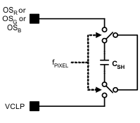 Figure 5. Equivalent Input Switched Capacitance S/H Mode
In Sample and Hold Mode, the impedance of the analog input pins is dominated by the switched capacitance of the CDS/Sample and Hold amplifier. The amplifier switched capacitance, shown as CS in Figure 4, and internal parasitic capacitances can be estimated by a single capacitor switched between the analog input and the VCLP reference pin for Sample and Hold mode. During each pixel cycle, the modeled capacitor, CSH, is charged to the OSX-VCLP voltage then discharged. The average input current at the OSX pin can be calculated knowing the input signal amplitude and the frequency of the pixel. If the application requires AC coupling of the CCD output to the LM98714 analog inputs, the Sample and Hold Mode input bias current may degrade the DC bias point of the coupling capacitor. To overcome this, Input Source Follower Buffers are available to isolate the larger Sample and Hold Mode input bias currents from the analog input pin (as discussed in the following section). As shown in Figure 6, the input bias current is much lower for CDS mode, eliminating the need for the source follower buffers.
7.3.3.1 CDS Mode
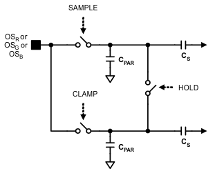 Figure 6. CDS Mode Simplified Input Diagram
Correlated Double Sampling mode does not require as precise a DC bias point as does Sample and Hold mode. This is due mainly to the nature of CDS itself, that is, the Video Signal voltage is referenced to the Reset Level voltage instead of the static DC VCLP voltage. The common mode voltage of these two points on the CCD waveform have little bearing on the resulting differential result. However, the DC bias point does need to be established to ensure the CCD waveform’s common mode voltage is within rated operating ranges.
The CDS mode biasing can be performed in the same way as described in the Sample/Hold Mode Biasing section, or, an alternative method is available which precludes the need for a CLPIN pulse. Internal resistor dividers can be switched in across the OSR, OSG, and/or OSB inputs to provide the DC bias voltage.
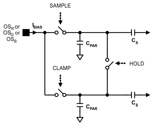 Figure 7. CDS Mode Input Bias Current
Unlike in Sample and Hold Mode, the input bias current in CDS Mode is relatively small. Due to the architecture of CDS switching, the average charge loss or gain on the input node is ideally zero over the duration of a pixel. This results in a much lower input bias current, whose main source is parasitic impedances and leakage currents. As a result of the lower input bias current in CDS Mode, maintaining the DC Bias point the input node over the length of a line will require a much smaller AC input coupling capacitor.
7.3.3.2 Input Source Follower Buffers
The OSR, OSG, OSB inputs each have an optional Source Follower Buffer which can be selected with Main Configuration Register 1, Bit[7]. These source followers provide a much higher impedance seen at the inputs. In some configurations, such as Sample and Hold Mode with AC coupled inputs, the DC bias point of the input nodes must remain as constant as possible over the entire length of the line to ensure a uniform comparison to reference level (VCLP in this case). The Source Followers effectively isolate the AC input coupling capacitor from the switched capacitor network internal to the LM98714’s Sample and Hold/CDS Amplifier. This results in a greatly reduced charge loss or gain on the AC Input coupling capacitor over the length of a line, thereby preserving its DC bias point.
The Source Followers should only be used in the 1.2 V input range (i.e. Main Configuration Register 2, Bit[4] = 1, CDS Gain = 2x). Using the Source Followers in the 2.4 V (i.e. Main Configuration Register 2, Bit[4] = 0, CDS Gain = 1x). input range will result in a loss of performance (mainly linearity performance at the high and low ends of the input range).
7.3.3.3 VCLP DAC
The VCLP pin provides the reference level for incoming signals in Sample and Hold Mode. The pin’s voltage can be set by one of three sources by writing to the VCLP Configuration Register on register page 0. By default, the VCLP pin voltage is established by an internal resistor divider which sets the voltage to VA/2. The resistor ladder can be disconnected and the pin driven externally by the application.
The most flexible method of setting the VCLP voltage is using the internal VCLP DAC buffer. The DAC is connected by setting the VCLP Configuration register Bit[5:4] to 2b’01. The DAC has a four bit “offset binary” format which is summarized in Table 2. The DAC output has an approximate swing of ±1.2 V.
Table 2. VCLP DAC Format
| VCLP Configuration [3:0] | Typical VCLP Output |
|---|---|
| 0 | -Full Scale |
| 0111 | Mid Scale - LSB |
| 1000 | Mid Scale |
| 1001 | Mid Scale + 1 LSB |
| 1111 | +Full Scale |
7.3.4 Coarse Pixel Phase Alignment
Precise placement of the CCD video signal sampling point is a critical aspect in any typical imaging application. Many factors such as logic gate propagation delays and signal skew increase the difficulty in properly aligning the CCD pixel output signals with the AFE input sampling points. The LM98714 provides two powerful features to aid the system level designer in properly sampling the CCD video signal under a large range of conditions. The first feature, discussed in this section, is the Coarse Pixel Phase Alignment block. As the name implies, this block provides a very coarse range of timing adjustment to align the phase of the CCD Pixel output with the phase of the LM98714 sample circuit. The second feature, discussed on the Internal Sample Timing section, is the block which is designed for fine tuning of the sampling points within the selected Coarse Pixel Alignment Phase. A small portion of a typical imaging application is shown in Figure 8.
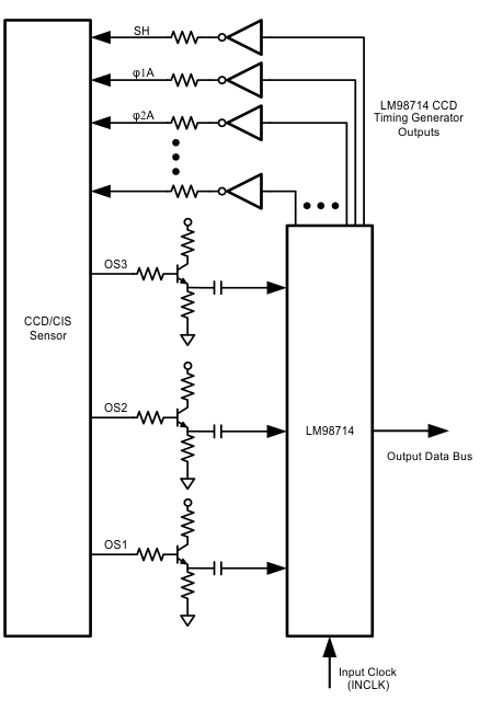 Figure 8. Typical AFE/CCD Interface
As shown in the diagram, the LM98714 provides the timing signals to drive the CCD using external logic gates to drive the high capacitance CCD clock pins. The pixels are shifted out of the CCD, through the emitter follower buffers and received by the LM98714 inputs for processing.
In an ideal application, depicted in Figure 9, the Pixel output signal would be in phase with the timing signals that drove the CCD. The LM98714 input sampling clocks (CLAMP and SAMPLE) are adjustable within a pixel period. By default, the pixel period (or pixel “phase”) is defined to be in line with the input clock. As shown in the ideal case in Figure 9, CLAMP and SAMPLE can be properly adjusted to their ideal positions within the pixel phase, shown below at the stable region near the end of the pedestal and data phases.
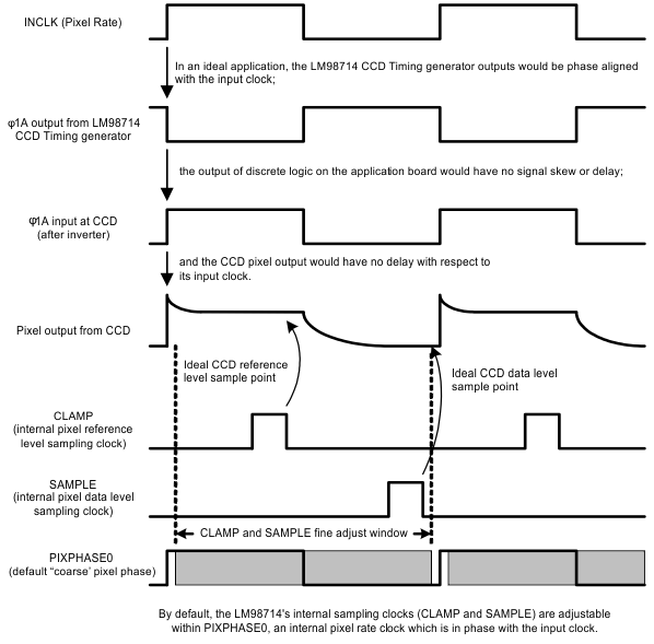 Figure 9. Clock Alignment in an Ideal Application
In a real system however, propagation delays exist in all stages of the signal chain. These propagation delays will lead to a shift in the CCD Pixel outputs with respect to the LM98714 input clock. The phase shift of the CCD Pixel output, demonstrated in Figure 10, can lead to significant sample timing issues if not properly corrected.
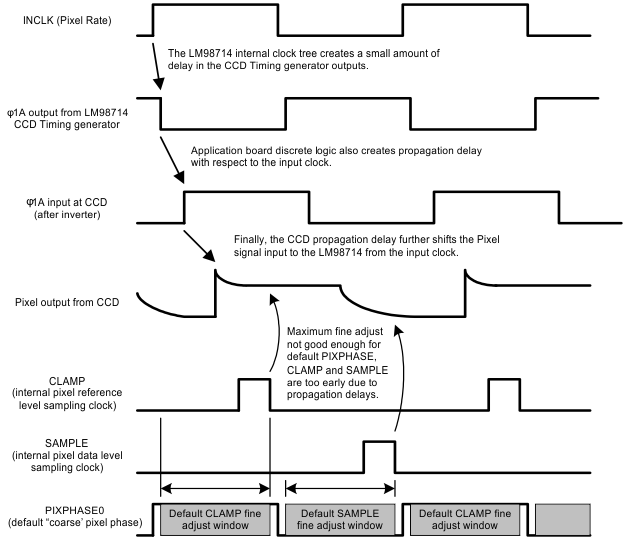 Figure 10. CCD Output Phase Shift in a Real Application
In the default mode, the LM98714 sampling is performed during a clock period whose phase is aligned with the input clock (ignoring any clock tree skew for the moment). The actual sampling clocks are adjustable within the clock period, as shown in Figure 10 (shown for CDS mode in the diagram) and further described in the Internal Sample Timing section. As shown in the diagram, the delay of the CCD Pixel output is shifted far enough that the fine CLAMP and SAMPLE clocks cannot be placed in a stable portion of the waveform. To remedy this situation, the LM98714’s Coarse Pixel Phase Alignment feature allows the designer to shift the entire phase of the analog front end with respect to the input clock. This allows the designer to choose one of four sampling phases which best matches the delay in the external circuitry. Once the “Coarse Pixel Phase” has been chosen, the designer can then fine tune the sampling clocks using the fine adjustment (see Internal Sample Timing).
The four available Coarse Pixel Phases (PIXPHASE0 - PIXPHASE3) are depicted in Figure 11 (Mode 3), Figure 12 (Mode 2) and Figure 13 (Mode 1). Also shown in the diagrams are the external input clock (INCLK) and a typical CCD output delayed from the input clock.
7.3.5 Internal Sample Timing
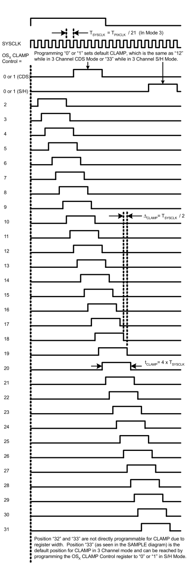
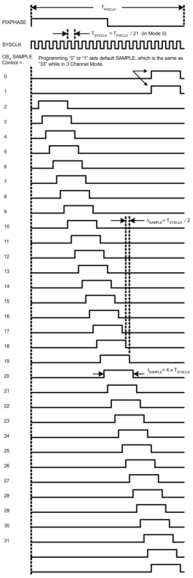
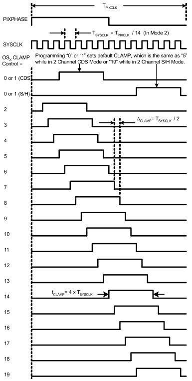
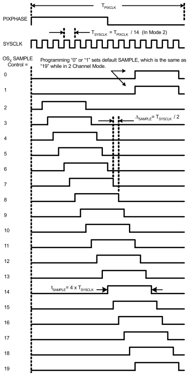
A typical CCD input signal is depicted in Figure 14 and Figure 15. Also shown are the internally generated SAMPLE and CLAMP pulses. These signals provide the sampling points of the input signal (OSX). The timing of SAMPLE and CLAMP is derived from an internal system clock (SYSCLK).
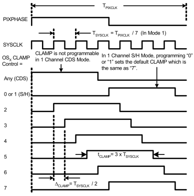
The pixel’s reference level input (depicted as VREF) is captured by the falling edge of the CLAMP pulse. In Sample/Hold Mode the VREF input is a sample of the VCLP DC voltage. In CDS Mode the CLAMP pulse samples the pedestal Level of the CCD output waveform.
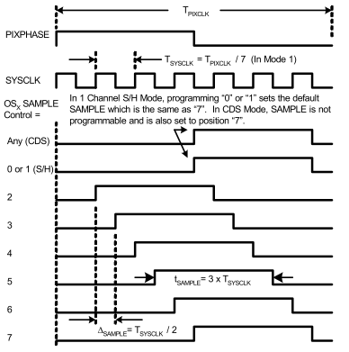
The pixel’s signal level input (depicted as VSIG) is captured by the SAMPLE pulse. In either Sample/Hold or CDS Mode, the VSIG input is the signal level of the CCD output waveform.
The LM98714 provides fine adjustment of the CLAMP and SAMPLE pulse placement within the pixel period. This allows the user to program the optimum location of the CLAMP and SAMPLE falling edges. In CDS mode, both CLAMP and SAMPLE are independently adjustable for each channel in use. In Sample/Hold mode, CLAMP is coincident with SAMPLE by default, but is also independently adjustable. The available fine tuning locations for CLAMP and SAMPLE are shown in Figure 16 through Figure 21 for each sampling mode (CDS or S/H) and channel mode (3, 2, or 1 Channel).
7.3.6 Automatic Black Level Correction Loop
CCD signal processors require a reference level for the proper handling of input signals; this reference level is commonly referred to as the black level. The LM98714 provides an Automatic Black Level Correction Loop as shown in Figure 22. The timing for this function is shown in Figure 23. The loop can be disabled and the Black Level Offset DAC registers programmed manually if desired.
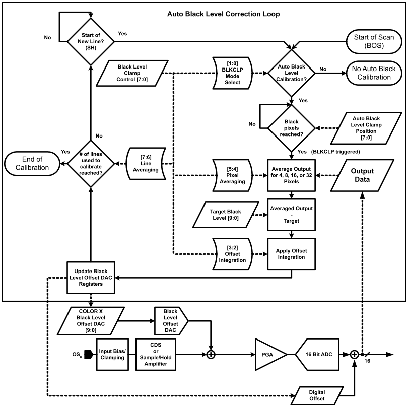 Figure 22. Black Level Correction Loop
The loop is intended to be used prior to scanning the page or during the first several lines at the beginning of a scan. The loop calibrates the channel offset such that the ADC outputs the desired code for Optical Black Pixels. In automatic mode, the pixels used to calibrate the offset should be Optical Black pixels represented by the internal “BLKCLP” pulse in Figure 23.
7.3.6.1 Black Level Offset DAC
The offset level registers store the DAC value required to meet the respective channel’s black level output. While using the Auto Black Level Correction Loop, the DAC registers are re-written as required every line the loop is enabled.
7.3.6.2 Black Level Clamp (BLKCLP)
The BLKCLP pulse can be synchronized by either the falling edge of the SH pulse or the CLPIN pulse (both shown in Figure 23). The automatic BLKCLP pulse will begin “n” number of pixel periods after the falling edge of the reference pulse where “n” is the Auto Black Level Clamp Position register. The reference point is programmed by the BLKCLP Mode Select Bits[1:0] within the Black Level Clamp Control register. The BLKCLP pulse should not be programmed coincident to the CLPIN pulse (if the CLPIN pulse is being used).
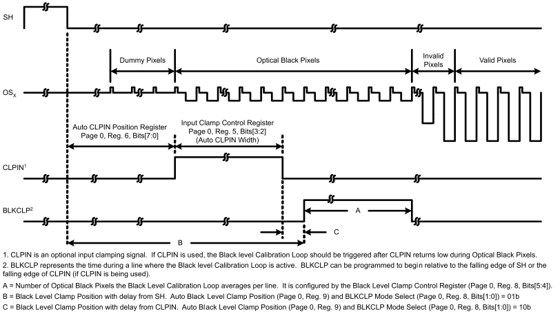 Figure 23. Black Level Correction Timing
7.3.6.3 Pixel Averaging
In order to obtain a snapshot of the current value for black (for comparison with the desired level of black) the ADC output is sampled upon activation of BLKCLP. Since a single optical black pixel is unlikely to be an accurate representation of the black level, a number of adjacent pixels are averaged. The number of pixels sampled is programmable by the Pixel Averaging Bit[5:4] within the Black Level Clamp Control register. The ability to select the number of pixels to be averaged (4, 8, 16, or 32 per line) provides greater flexibility allowing the LM98714 to be used with different CCDs having differing number of black pixels.
7.3.6.4 Target Black Level
The Target Black Level registers define a 10-bit word that specifies an ADC output (on the 12 bit level) corresponding to the desired optical black output code (ignoring the four LSBs of the 16 Bit ADC output). In other words, one Target Black Level LSB corresponds to sixteen ADC LSBs. Assertion of the BLKCLP signal activates the digital black clamp loop and the black level is steered toward the value stored in the output black level register. The digital black clamp loop is only limited in it’s range by the offset DAC’s range.
Once the correct number of pixels have been averaged, the value is subtracted from the Target Black Level and an error value is produced.
7.3.6.5 Offset Integration
Each time the BLKCLP signal is activated, the average ADC output of several black pixels is compared to the Target Black Level producing an error value. This error value is not directly added (or subtracted) to the Black Level Offset register, rather, the value applied is a programmable fraction of this error. This has the effect of slowing down the offset convergence resulting in a calculation for offset that is less susceptible to noise. The scaling factor is stored in the Offset integration Bits[3:2] of the Black Level Clamp Control register. The scaling values are divided-by-8, 16, 32, or 64. Divide-by-8 provides the quickest convergence of the loop (for use when the number of lines available for calibration is limited) and Divide-by-64 the longest (for use when using an large number of lines to converge).
7.3.6.6 Line Averaging
The Auto Black level Correction Loop can be run for 15 lines, 31 lines, 63 lines, or infinite (every line). The Line Averaging Bits[7:6] found in the lack Level Clamp Control register set the number of lines that the loop will run after the Start of Scan. The recommended use of the Auto Black Level Correction Loop is in a calibration period prior to moving the sensor down the page or during the first several lines of the page. By experimenting with the Line Averaging and Offset Integration bits with no sensor illumination (black pixels), the proper settings for the Auto Black Level Correction Loop are determined when the ADC output converges to the Target Black Level value. If the loop converges with the 15, 31, or 63 line setting, the loop can remain enabled. The loop does not update the Black Level Offset DAC once the number of lines since “Start of Scan” has passed. If the loop requires more than 63 lines to converge (i.e. requires Line Averaging = infinite), it is recommended to disable the loop after convergence has been reached. In the “infinite” setting, the loop will continuously update the Black Level Offset registers as long as the loop is enabled throughout the entire scan.
7.3.7 Internal Timing Generation
A flexible internal timing generator is included to provide clocking signals to CCD and CIS sensors. A block diagram of the CCD Timing Generator is shown in Figure 24.
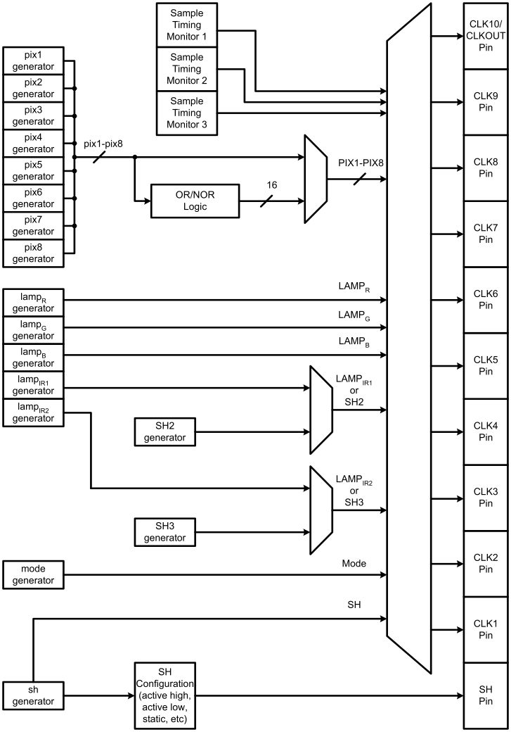 Figure 24. CCD Timing Generator Block Diagram
Examples of the various operating modes and settings are shown following. The detailed pixel timing is somewhat dependent on the operating modes of the AFE circuitry regarding the number of adjustment points for the on and off points of the different timing outputs.
NOTE
In addition to the timing adjustments shown, the polarity of all sensor clock signals can be adjusted by register control.
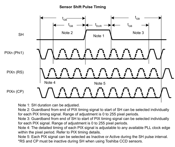 Figure 27. Sensor Timing SH Pulse Details
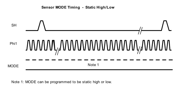 Figure 28. Sensor Timing Mode Pin Output Details - Static High/Low
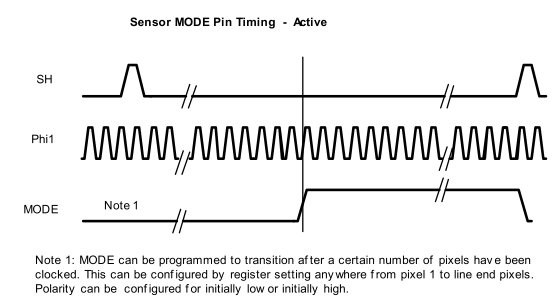 Figure 29. Sensor Timing Mode Pin Output Details - Active Programmed Transition
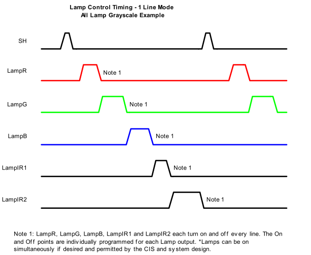 Figure 30. Lamp Control Timing - 1 Line Mode (Monochrome)
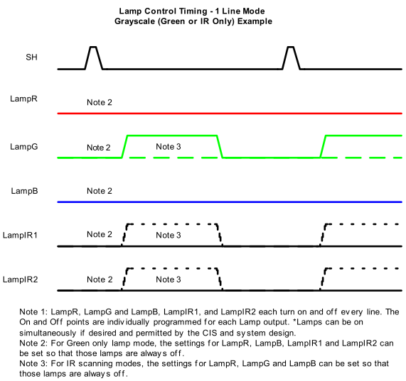 Figure 31. Lamp Control Timing - 1 Line Mode
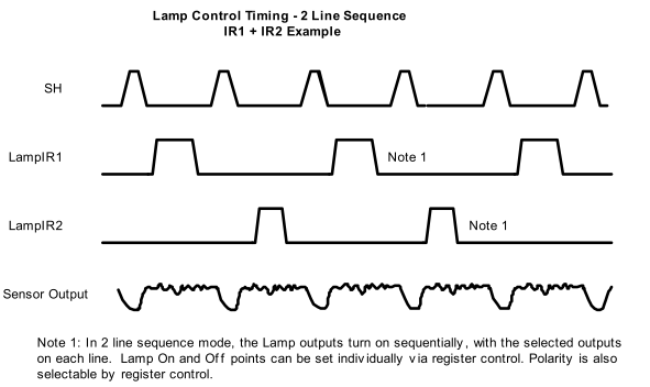 Figure 32. Lamp Control Timing - 2 Line Sequence
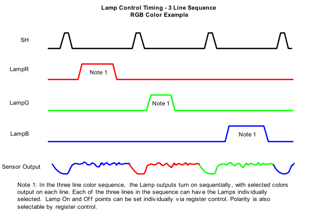 Figure 33. Lamp Control Timing - 3 Line Sequence
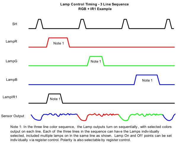 Figure 34. Lamp Control Timing - 3 Line Sequence - IR Enhancement Example
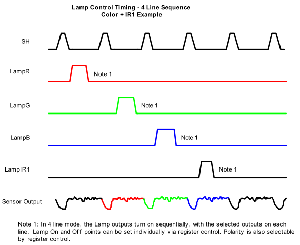 Figure 35. Lamp Control Timing - 4 Line Sequence
Color + IR1 Example
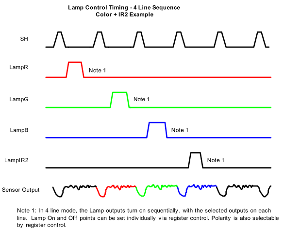 Figure 36. Lamp Control Timing - 4 Line Sequence
Color + IR2 Example
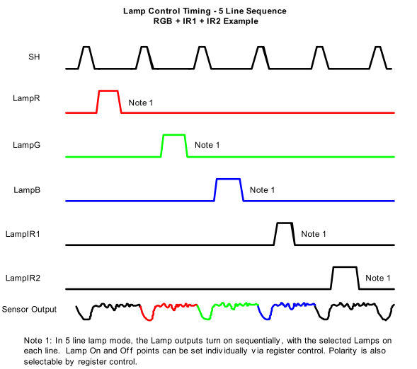 Figure 37. Lamp Control Timing - 5 Line Sequence
7.3.7.1 Pix Signal Generator OR/NOR Modes
As shown in Figure 24, the PIX signal generators outputs can be used in their normal form and sent to the LM98714 output pins, or, they can be sent through an additional layer of OR and NOR logic to provide a number of clocking variations. The OR and NOR combinations of multiple PIX signals can be useful for such modes as pixel lumping, or other modes where more complicated phi clocks are required.
The OR and NOR functions are chosen through the PIX OR/NOR Control 1 and PIX OR/NOR Control 2 registers on Page 4 of the serial interface register map. When all of the OR/NOR control bits are 0 (default) the PIX signals are sent directly from the pix signal generators to the output pins configured by the Output Mapping Control registers (register Page 3). When an OR/NOR control bit is set to 1, the OR or NOR product of multiple pix signal generators is routed to the output pin described in the register details.
7.3.7.2 SH2 and SH3 Generation
In some sensors, there is a requirement for up to three “SH” type signals. The LM98714 CCD Timing Generator can be configured to produce optional SH signals as shown in Figure 38, these SH signals (SH2 and SH3) toggle every other line and are coincident with the original SH pulse.
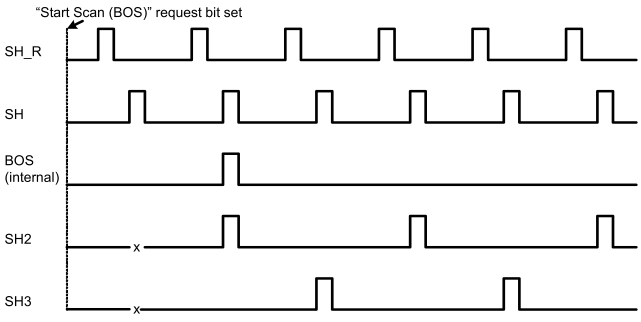 Figure 38. SH2 and SH3 Generation
The “Start Scan (BOS)” request bit is used to begin the proper sequence of CCD Timing outputs at the beginning of a scan. The first line of pixels are being processed by the CCD during the first integration period (after the first SH). The BOS signal (internal to the LM98714) occurs at the second SH to signal when the first line of pixels are actually shifting out of the CCD and in to the AFE. The SH2 pulse is synchronized with the BOS signal and continues to toggle on an every other line basis. The SH3 signal occurs on opposite lines from SH2.
The SH2 and SH3 signals are available in place of the Lamp IR1 and Lamp IR2 outputs respectively. The routing of SH2 and SH3 is depicted in Figure 24. The use of SH2 and SH3 is selected by the SH2/SH3 Control register (0x0F) on Page 4 of the register map.
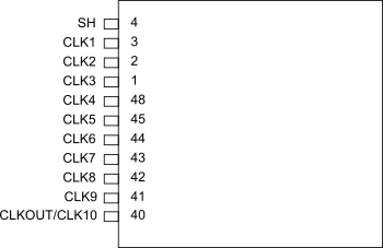 Figure 39. Sensor Control Outputs
Table 3 shows a number of example mappings of the sensor timing signals to the sensor control CLKn outputs. Several typical timings are shown here, but any timing generator signal can be mapped to any of the CLKn outputs, providing maximum flexibility.
Table 3. Sensor Timing Mappings Examples
| Sensor Control Output | Example A | Example B | Example C | Example D | Example E | Example F |
|---|---|---|---|---|---|---|
| SH | SH | SH | SH | SH | SH | SH |
| CLK1 | PIX1(PHI1) | PIX1(PHI1) | PIX1(PHI1) | PIX1(PHI1) | PIX1(PHI1) | PIX1(PHI1) |
| CLK2 | PIX2(PHI2) | PIX2(PHI2) | PIX2(PHI2) | PIX2(PHI2) | PIX2(PHI2) | PIX2(PHI2) |
| CLK3 | PIX3(RS) | PIX3(RS) | PIX3(RS) | PIX3(RS) | PIX3(PHI3) | PIX3(RS) |
| CLK4 | PIX4(CP) | PIX4(CP) | LAMPR | PIX4(CP) | PIX4(PHI4) | PIX4(CP) |
| CLK5 | LAMPR | LAMPR | LAMPG | LAMPR | PIX5(PHI5) | CB[0] |
| CLK6 | LAMPG | LAMPG | LAMPB | LAMPG | PIX6(PHI6) | CB[1] |
| CLK7 | LAMPB | LAMPB | LAMPIR1 | LAMPB | PIX7(RS) | CB[2] |
| CLK8 | MODE | LAMPIR1 | LAMPIR2 | LAMPIR1 | PIX8(CP) | CB[3] |
| CLK9 | PIX5(PHI3) | LAMPIR2 | MODE | LAMPIR2 | MODE | CB[4] |
| CLKOUT/CLK10 | (MODE) | PIX5(PHI3) | CLKOUT |
These examples can be used for any customer need, but typical applications would be as follows:
In Examples A, B and C, only 10 sensor control outputs are used. This is to allow the CLKOUT/CLK10 pin to be used as a timing reference for the image output data when the outputs are in CMOS mode.
Example A: Used with most CCD or CIS sensors, including new sensors with 3 PHI clock inputs. Will support up to 3 color LED lamps. Supports CCD sensors with switchable resolution through the MODE control output.
Example B: Used in applications where up to 2 additional IR lamps are used in addition to the R, G, B lamps. No resolution MODE output is available.
Example C: Used where no CP pulse is needed, but 5 lamp outputs are needed as well as a MODE sensor resolution control pin.
In Examples D and E, the CLK10 output is also used. These modes are not available when the image data outputs are operating in CMOS mode.
Example D: Provides both PHI3 output and 5 LED lamp outputs. Does not provide MODE output for resolution control.
Example E: Provides 5 LED lamp outputs, and the MODE output for sensor resolution control.
7.3.8 CCD Timing Generator Master/Slave Modes
The internal CCD Timing generator is capable of operating in Master Mode or in Slave Mode. The Master/Slave operation is configured with the SH Mode Register (Register 0x00 on Page 2). In either Master or Slave Mode, control bit data can be sent to the output of the LM98714 to indicate when each new scan is starting as well as pixel information such as color, type (active, black, dummy, etc.), and the beginning of each line.
7.3.8.1 Master Timing Generator Mode
In Master Timing Mode, the LM98714 controls the entire CCD Timing Generator based on a Start Scan Bit (Main Configuration Register 2, Bit[0] is the “Start Scan” or “BOS/Beginning of Scan” bit). The Start Scan bit is set by the user to request a new scan. This bit is a self clearing register bit written to the serial interface. When received, the LM98714 controls where and when each new line of the scan begins and ends based on the CCD Timing Generator register settings. The scan is enabled as long as the Active/Standby bit is low. The period of the line (integration time) is controlled by the SH Width setting (SH Pulse Width Register) and the Line End setting (Line End MSB and Line End LSB registers).
7.3.8.2 Slave Timing Generator Mode
In Slave Timing Mode, the LM98714 CCD Timing Generator is controlled by the external SH_R pin. Each new line of a scan is initiated by an SH_R pulse. The period of the line (integration time) is mainly controlled by the period of the incoming SH_R signal.
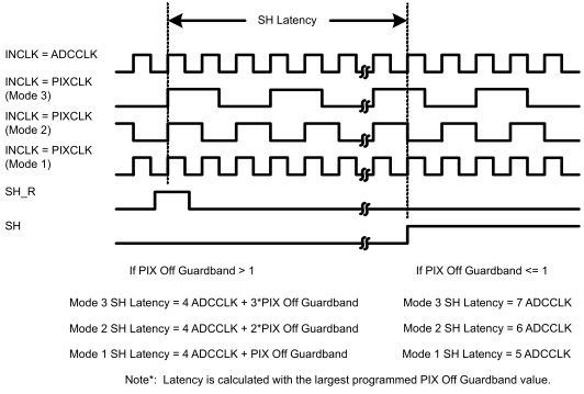 Figure 40. SH_R Input to SH Output Latency Diagram
 Figure 41. SH_R to INCLK (PIXCLK or ADCCLK) Timing
7.3.9 LVDS Output Mode
7.3.9.1 LVDS Output Format
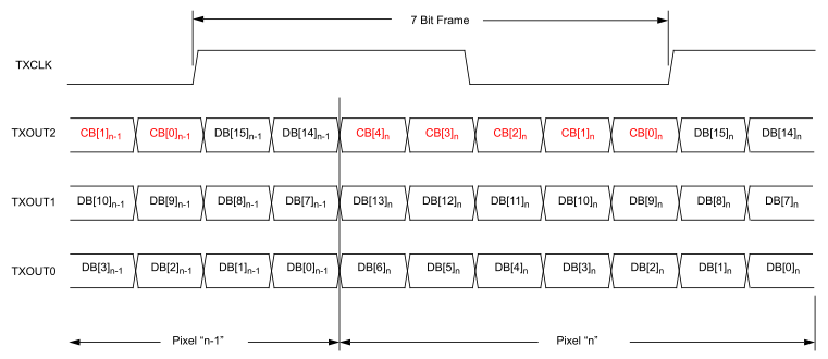 Figure 43. LVDS Output Bit Alignment and Data Format
7.3.9.2 LVDS Output Timing Details
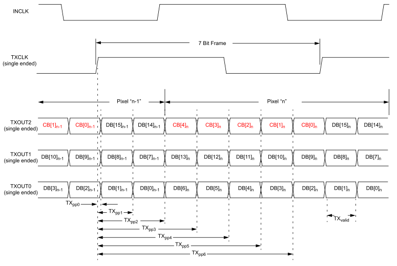 Figure 44. LVDS Data Output Mode Specification Diagram
7.3.9.3 LVDS Control Bit Coding
The 5 control bits included in the LVDS data stream are coded as follows:
The "active" and "black" pixel tags are programmable tags that the LM98714 provides in order to identify how many pixels have been processed since the falling edge of SH.
Which pixels are given "active" and "black" CB tags is controlled by Page 4, registers 0x08 through 0x0D (Optical Black Pixels Start, Optical Black Pixels End, Start of Valid Pixels, and End of Valid Pixels).
The LM98714 counts the number of pixel periods after the falling edge of SH: If the number of pixel periods after the falling edge of SH is between "optical black pixels start" and "optical black pixels end" the CB bits will indicate that the pixel is a black pixel. If the number of pixel periods after the falling edge of SH is between "start of valid pixels" and "end of valid pixels" the CB bits will indicate that the pixel is an active pixel.
Table 4.
| CB[4] | Description |
|---|---|
| 0 | Not the beginning of line |
| 1 | Beginning of Line |
| (This bit is high for as many pixels as SH pulse is active) |
Table 5.
| CB[3:0] | Description |
|---|---|
| 0 | Dummy Pixels |
| 1 | Red Active Pixels |
| 10 | Green Active Pixels |
| 11 | Blue Active Pixels |
| 100 | IR1 Active Pixels |
| 101 | IR2 Active Pixels |
| 110 | Red Black Pixels |
| 111 | Green Black Pixels |
| 1000 | Blue Black Pixels |
| 1001 | IR1 Black Pixels |
| 1010 | IR2 Black Pixels |
| 1111 | Beginning of Scan |
7.3.9.4 LVDS Data Latency Diagrams
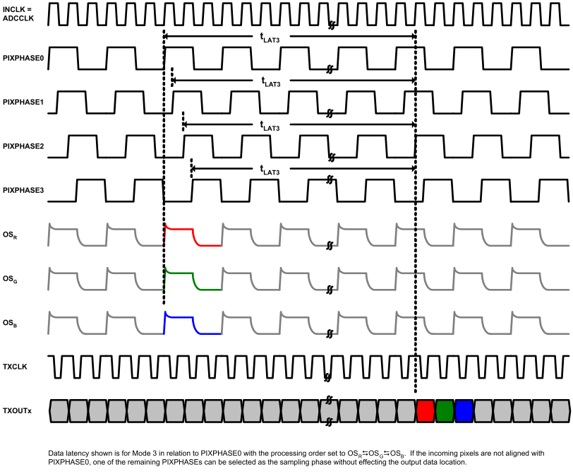 Figure 45. Mode 3 LVDS Data Latency
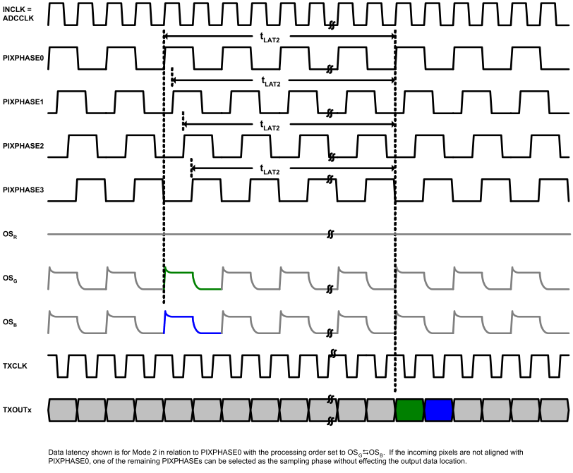 Figure 46. Mode 2 LVDS Data Latency
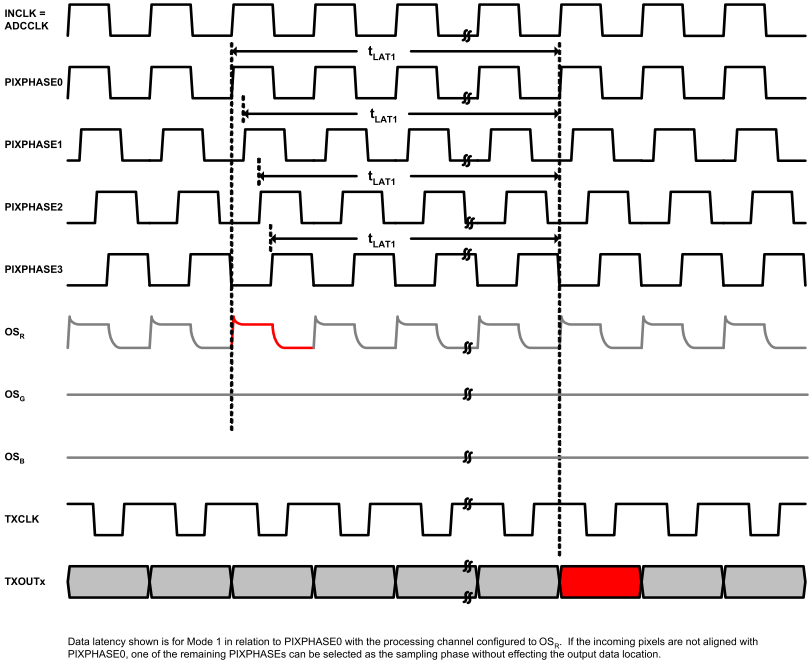 Figure 47. Mode 1 LVDS Data Latency
7.3.9.5 LVDS Test Modes
The LVDS test modes present several different data patterns to the input of the LVDS serializer block. All 21 bits are used and there is no control bit coding present. The SH signal resets the LVDS test pattern and the pattern will resume only after SH is deasserted. If no SH signal is sent, the pattern continues indefinitely.
7.3.9.5.1 Test Mode 1 - Worst Case Transitions
This test mode provides an LVDS output with the maximum possible transitions. This mode is useful for system EMI evaluations, and for ATE timing tests.
The effective data values are an alternating pattern between 21’b101010101010101010101 (0x155555) and 21’b010101010101010101010 (0x0AAAAA). This test pattern resets to 0x155555 after the SH signal.
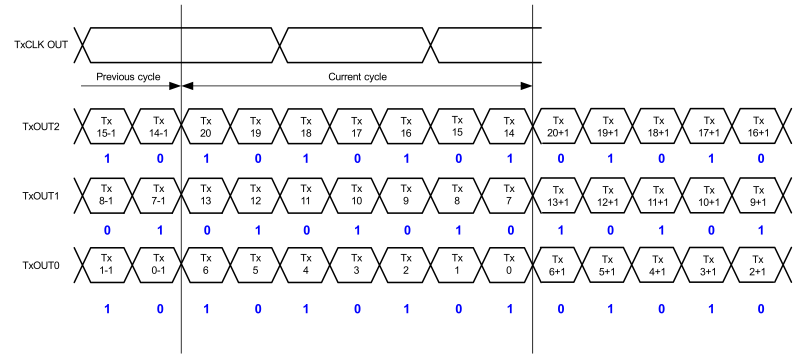 Figure 48. LVDS Test Pattern
7.3.9.5.2 Test Mode 2 - Ramp
This mode provides LVDS data that progresses from 0x00000 to the full scale output 0x1FFFFF incrementing by 1 per LVDS Clock. When the LVDS ramp test pattern is selected, the ramp begins immediately and counts from zero to the full scale value, and then repeats.
7.3.9.5.3 Test Mode 3 - Fixed Output Data
This mode allows a fixed data value to be output. The value is set via. Upcounter Register 1, 2 and 3. The 21 bit value taken from these registers is repetitively sent out over the LVDS link. This is useful for system debugging of the LVDS link and receiver circuitry.
7.3.10 CMOS Output Mode
7.3.10.1 CMOS Output Data Format
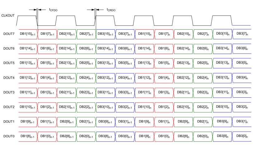 Figure 49. CMOS Data Output Format (Mode 3 Shown)
7.3.11 CMOS Output Data Latency Diagrams
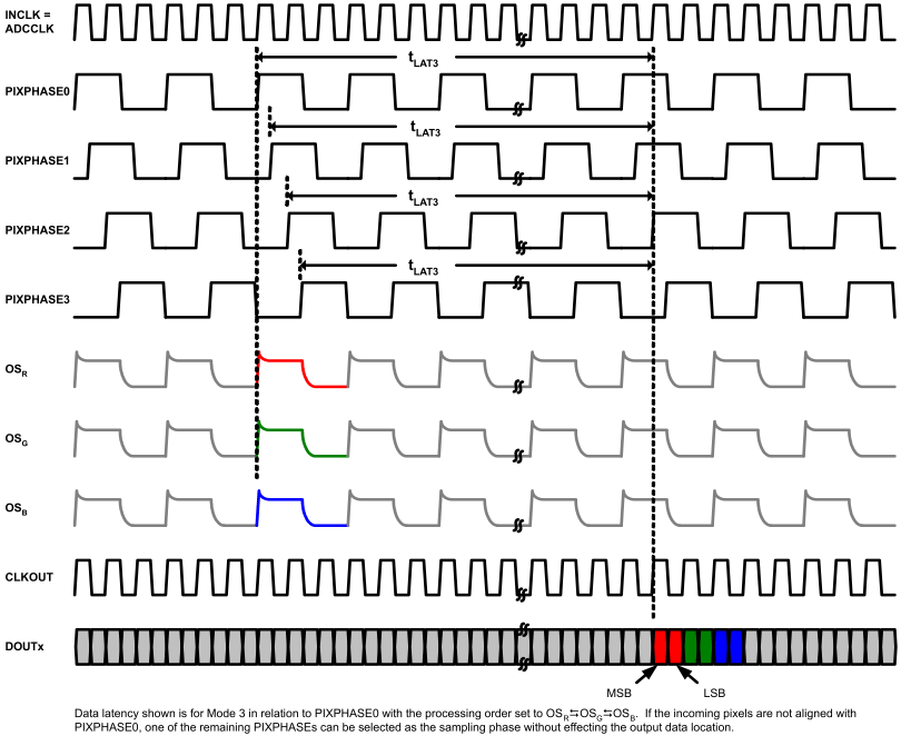 Figure 50. Mode 3 CMOS Output Latency
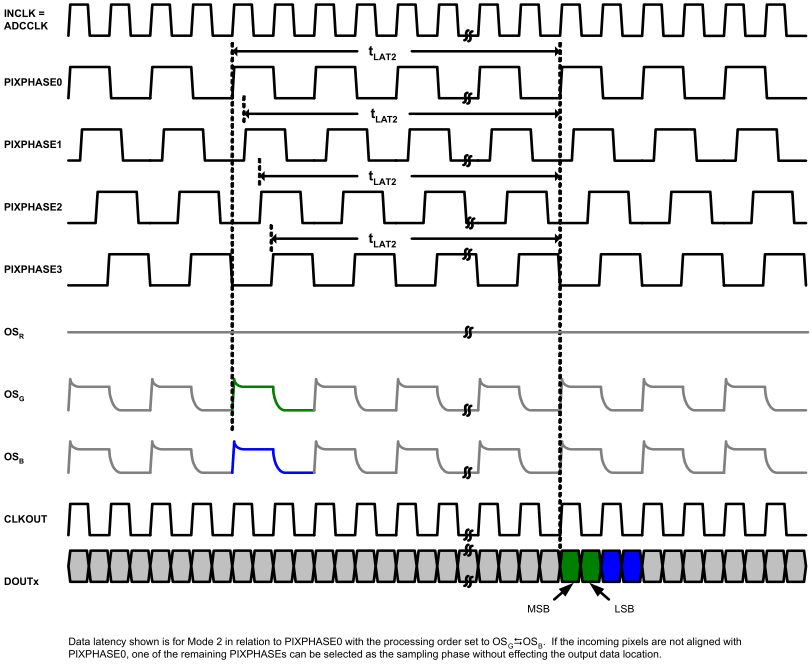 Figure 51. Mode 2 CMOS Output Latency
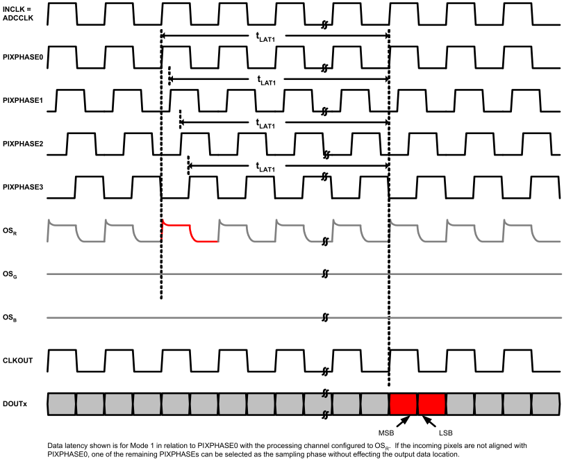 Figure 52. Mode 1 CMOS Output Latency
7.4 Device Functional Modes
Table 6 lists the register settings for the modes of operation.
Table 6. Modes Of Operation Register Settings Table
| Operating Mode | Sampling Input | Signal Path | Output Sequencing Mode 3 and 2 = Pixel Seq Mode 1 = Color Line Seq |
Main Config. |
Main Config. Register 0 | |||||||
|---|---|---|---|---|---|---|---|---|---|---|---|---|
| Reg. 3 | Mode | Color | Order | Color Seq. Length | ||||||||
| Bit [3] | Bit[7] | Bit[6] | Bit[5] | Bit[4] | Bit[3] | Bit[2] | Bit[1] | Bit[0] | ||||
| Mode3-RGB Forward | OSR||OSG||OSB | RGB | PixelR→PixelG→PixelB→ | x | 1 | 1 | 1 | 1 | 0 | 0 | 0 | 1 |
| Mode3-RGB Reverse | OSR||OSG||OSB | RGB | PixelB→PixelG→PixelR→ | x | 1 | 1 | 1 | 1 | 1 | 0 | 0 | 1 |
| Mode2-RG Forw. | OSR||OSG | RG | PixelR→PixelG→ | x | 1 | 0 | 0 | 0 | 0 | 0 | 0 | 1 |
| Mode2-RG Rev. | OSR||OSG | RG | PixelG→PixelR→ | x | 1 | 0 | 0 | 0 | 1 | 0 | 0 | 1 |
| Mode2-GB Forw. | OSG||OSB | GB | PixelG→PixelB→ | x | 1 | 0 | 0 | 1 | 0 | 0 | 0 | 1 |
| Mode2-GB Rev. | OSG||OSB | GB | PixelB→PixelG→ | x | 1 | 0 | 0 | 1 | 1 | 0 | 0 | 1 |
| Mode2-RB Forw. | OSR||OSB | RB | PixelR→PixelB→ | x | 1 | 0 | 1 | 0 | 0 | 0 | 0 | 1 |
| Mode2-RB Rev. | OSR||OSB | RB | PixelB→PixelR→ | x | 1 | 0 | 1 | 0 | 1 | 0 | 0 | 1 |
| Mode1-R Mono | OSR | R | Color Line Seq: 1→1→1→1→1→ | x | 0 | 1 | 0 | 0 | 0 | 0 | 0 | 1 |
| Mode1a-R 2 Color For. | OSR | R | Color Line Seq: 1→2→1→2→1→ | 0 | 0 | 1 | 0 | 0 | 0 | 0 | 1 | 0 |
| Mode1a-R 2 Color Rev | OSR | R | Color Line Seq: 2→1→2→1→2→ | 0 | 0 | 1 | 0 | 0 | 1 | 0 | 1 | 0 |
| Mode1a-R 3 Color For. | OSR | R | Color Line Seq: 1→2→3→1→2→ | 0 | 0 | 1 | 0 | 0 | 0 | 0 | 1 | 1 |
| Mode1a-R 3 Color Rev | OSR | R | Color Line Seq: 3→2→1→3→2→ | 0 | 0 | 1 | 0 | 0 | 1 | 0 | 1 | 1 |
| Mode1a-R 4 Color For. | OSR | R | Color Line Seq: 1→2→3→4→1→ | 0 | 0 | 1 | 0 | 0 | 0 | 1 | 0 | 0 |
| Mode1a-R 4 Color Rev | OSR | R | Color Line Seq: 4→3→2→1→4→ | 0 | 0 | 1 | 0 | 0 | 1 | 1 | 0 | 0 |
| Mode1a-R 5 Color For. | OSR | R | Color Line Seq: 1→2→3→4→5→ | 0 | 0 | 1 | 0 | 0 | 0 | 1 | 0 | 1 |
| Mode1a-R 5 Color Rev | OSR | R | Color Line Seq: 5→4→3→2→1→ | 0 | 0 | 1 | 0 | 0 | 1 | 1 | 0 | 1 |
| Mode1a-G Mono | OSG | G | Color Line Seq: 1→1→1→1→1→ | 1 | 0 | 1 | 0 | 1 | 0 | 0 | 0 | 1 |
| Mode1a-B Mono | OSB | B | Color Line Seq: 1→1→1→1→1→ | 1 | 0 | 1 | 1 | 0 | 0 | 0 | 0 | 1 |
| Mode1b-RGB Forward | OSR→OSG→OSB | RGB | LineR→LineG→LineB→ | 1 | 0 | 0 | 1 | 1 | 0 | x | x | x |
| Mode1b-RGB Reverse | OSB→OSG→OSR | RGB | LineR→LineG→LineB→ | 1 | 0 | 0 | 1 | 1 | 1 | x | x | x |
7.4.1 Mode 3 - Three Channel Input/Synchronous Pixel Sampling
In Mode 3, the OSR, OSG, and OSB input channels are sampled synchronously. The sampled input signals are then processed in parallel through their respective channels with each channel offset and gain adjusted by their respective control registers. The signals are then routed through a 3-1 MUX to the ADC. The order in which pixels are processed through the MUX to the ADC is programmable (OSR-OSG-OSB, or OSB-OSG-OSR) and is synchronized by the SH pulse.
Table 7. Mode 3 Operating Details
| Detail | |||
|---|---|---|---|
| Channels Active | OSB & OSG & OSR | 3 channel synchronous pixel sampling. | |
| Channel Sample Rate | 15 | MSPS per Channel (max) | |
| ADC Sample Rate | 45 | MSPS (max) | |
| fADC: fINCLK | Internal 3x Clock Selected | 3:01 | fINCLK = 15 MHz (max) |
| Internal 1x Clock Selected | 1:01 | fINCLK = 45 MHz (max) | |
| Output Sequencing | SH Signal --> R-G-B-R-G-B-R-G-B→ | ||
| or | |||
| SH Signal --> B-G-R-B-G-R-B-G-R→ | |||
7.4.2 Mode 2 - Two Channel Input/Synchronous Pixel Sampling
Mode 2 is useful for CCD sensors with a Black and White line with Even and Odd pixels. In its default configuration, Mode 2 samples Even sensor pixels via the Blue Channel Input, and Odd sensor pixels via the Green Channel Input. The selection of Even/Odd inputs can be changed through the serial interface registers. Sampling of the Even and Odd inputs is performed synchronously.
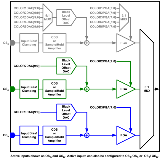 Figure 54. Mode 2 Signal Routing
Table 8. Mode 2 Operating Details
| Detail | |||
|---|---|---|---|
| Channels Active | OSG and OSB (Default) or OSR and OSG or OSB and OSR |
Two inputs synchronously processed as Even and Odd Pixels. Channel inputs are configurable. | |
| Channel Sample Rate | 22.5 | MSPS per Channel (max) | |
| ADC Sample Rate | 45 | MSPS (max) | |
| fADC: fINCLK | Internal 2x Clock Selected | 2:01 | fINCLK = 22.5 MHz (max) |
| Internal 1x Clock Selected | 1:01 | fINCLK = 45 MHz (max) | |
| Output Sequencing | SH Signal --> Even-Odd-Even-Odd-Even-Odd-Even→ or SH Signal --> Odd-Even-Odd-Even-Odd-Even-Odd→ |
||
7.4.3 Mode 1a - One Channel Input/One, Two, Three, Four, Or Five Color Sequential Line Sampling
In Mode 1a, all pixels are processed through a single input (OSR, OSG, or OSB) chosen through the control register setup. This mode is useful in applications where only one input channel is used. The selected input is programmable through the control register. If more than one color is being sent to the input, the user can configure the OSR channel to utilize up to five offset and gain coefficients for up to five different lines of color pixels. The SH pulse at the beginning of each line sequences the DAC and PGA coefficients as configured in the control registers. In this mode, the maximum channel speed is 30MSPS per channel with the ADC running at 30MSPS.
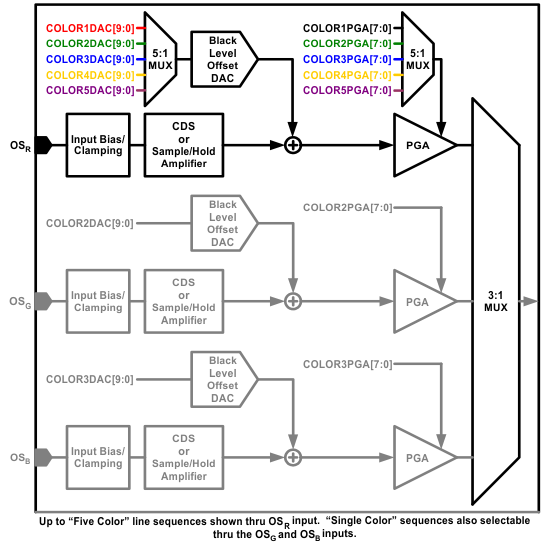 Figure 55. Mode 1a Signal Routing
Table 9. Mode 1a Operating Details
| Detail | |||
|---|---|---|---|
| Channels Active | OSR | One color active per line. | |
| Channel Sample Rate | 30 | MSPS per Channel (max) | |
| ADC Sample Rate | 30 | MSPS (max) | |
| fADC: fINCLK | Internal 1x Clock Selected | 1:01 | fINCLK = 30MHz (max) |
| Output Sequencing | SH Signal → Color 1→Color 1→Color 1→Color 1→Color 1→ | ||
| →SH Signal → Color 2→Color 2→Color 2→Color 2→Color 2→ | |||
| →SH Signal → Color 3→Color 3→Color 3→Color 3→Color 3→ | |||
| →SH Signal → Color 4→Color 4→Color 4→Color 4→Color 4→ | |||
| →SH Signal → Color 5→Color 5→Color 5→Color 5→Color 5→ | |||
| or | |||
| SH Signal → Color 5→Color 5→Color 5→Color 5→Color 5→ | |||
| →SH Signal → Color 4→Color 4→Color 4→Color 4→Color 4→ | |||
| →SH Signal → Color 3→Color 3→Color 3→Color 3→Color 3→ | |||
| →SH Signal → Color 2→Color 2→Color 2→Color 2→Color 2→ | |||
| →SH Signal → Color 1→Color 1→Color 1→Color 1→Color 1→ | |||
7.4.4 Mode 1b - One Channel Color Input Per Line/Sequential Line (Input) Sampling/Three Channel Processing
In Mode 1b, the OSR, OSG, and OSB inputs are sampled sequentially and processed through their respective channels. This mode allows an entire line of Red, Green, or Blue Pixels to be sampled before sequencing to the next input. This mode is useful with sensors that output whole lines of pixels of a single color. The order in which the channels are sampled is fully programmable. Actual switching from channel to channel is triggered by an SH pulse. The first SH pulse after this mode is set (or reset) sets up the first programmed channel for gain and offset and initiates sampling through that channel alone. The next SH pulse switches the active channel to the second channel indicated by the configuration registers. This sequencing with SH pulses continues to the third channel and then continuously loops through the channels.
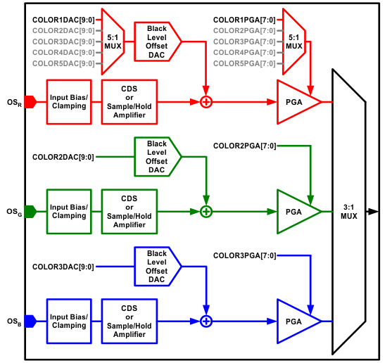 Figure 56. Mode 1b Signal Routing
Table 10. Mode 1b Operating Details
| Detail | |||
|---|---|---|---|
| Channels Active | OSB or OSG or OSR | One channel active per line. Active channel is sequenced by SH pulse at start of new line. | |
| Channel Sample Rate | 30 | MSPS per Channel (max) | |
| ADC Sample Rate | 30 | MSPS (max) | |
| fADC: fINCLK | Internal 1x Clock Selected | 1:01 | fINCLK = 30MHz (max) |
| Output Sequencing | SH Signal → R-R-R-R-R-R-R-R-R-R-R-R-R→ | ||
| →SH Signal → G-G-G-G-G-G-G-G-G-G-G-G-G→ | |||
| →SH Signal → B-B-B-B-B-B-B-B-B-B-B-B-B-B→ | |||
| or | |||
| SH Signal → B-B-B-B-B-B-B-B-B-B-B-B-B-B→ | |||
| →SH Signal → G-G-G-G-G-G-G-G-G-G-G-G-G→ | |||
| →SH Signal → R-R-R-R-R-R-R-R-R-R-R-R-R→ | |||
7.5 Programming
7.5.1 Serial Interface
A serial interface is used to write and read the configuration registers. The interface is a three wire interface using SCLK, SEN, and SDIO connections. The main input clock (INCLK) to the LM98714 must be active during all Serial Interface commands.
7.5.1.1 Writing To The Serial Registers
To write to the serial registers, the timing diagram shown in Figure 57 must be met. First, SEN is toggled low. The LM98714 assumes control of the SDIO pin during the first eight clocks of the command. During this period, data is clocked out of the device at the rising edge of SCLK. The eight bit value clocked out is the contents of the previously addressed register, regardless if the previous command was a read or a write. At the rising edge of ninth clock, the LM98714 releases control of the SDIO pin. At the falling edge of the ninth clock period, the master should assume control of the SDIO pin and begin issuing the new command. SDIO is clocked into the LM98714 at the rising edge of SCLK. The remaining bits are composed of the “write” command bit (a zero), two device address bits (zeros for the LM98714), five bit register address to be written, and the eight bit register value to be written. When SEN toggles high, the register is written to, and the LM98714 now functions with this new data.
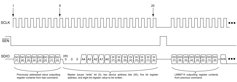 Figure 57. Serial Write
7.5.1.2 Reading The Serial Registers
To read to the serial registers, the timing diagram shown in Figure 58 must be met. First, SEN is toggled low. The LM98714 assumes control of the SDIO pin during the first eight clocks of the command. During this period, data is clocked out of the device at the rising edge of SCLK. The eight bit value clocked out is the contents of the previously addressed register, regardless if the previous command was a read or a write. At the rising edge of ninth clock, the LM98714 releases control of the SDIO pin. At the falling edge of the ninth clock period, the master should assume control of the SDIO pin and begin issuing the new command. SDIO is clocked into the LM98714 at the rising edge of SCLK. The remaining bits are composed of the “read” command bit (a one), two device address bits (zeros for the LM98714), five bit register address to be read, and the eight bit “don’t care” bits. When SEN toggles high, the register is not written to, but its contents are staged to be outputted at the beginning of the next command.
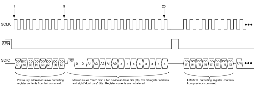 Figure 58. Serial Read
7.5.1.3 Serial Interface Timing Details
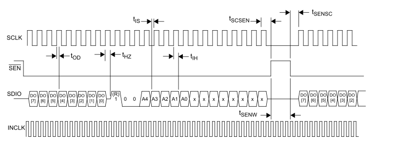 Figure 59. Serial Interface Specification Diagram
7.6 Register Maps
7.6.1 Configuration Registers
The LM98714 operation is very flexible to support a wide variety of sensors and system designs. This flexibility is controlled through configuration registers which are first summarized, then described in full in the following tables. Because the serial interface only allows 5 address bits, a register paging system is used to support the larger number of required registers.
A page register is present at the highest address (1Fh or 11111b). The power on default setting of the page register is 00. Writing other values to this register allows the other pages to be accessed. The page register is mirrored, and is accessible at the highest address on each page.
Figure 60 shows the proper sequence of operation for the LM98714.
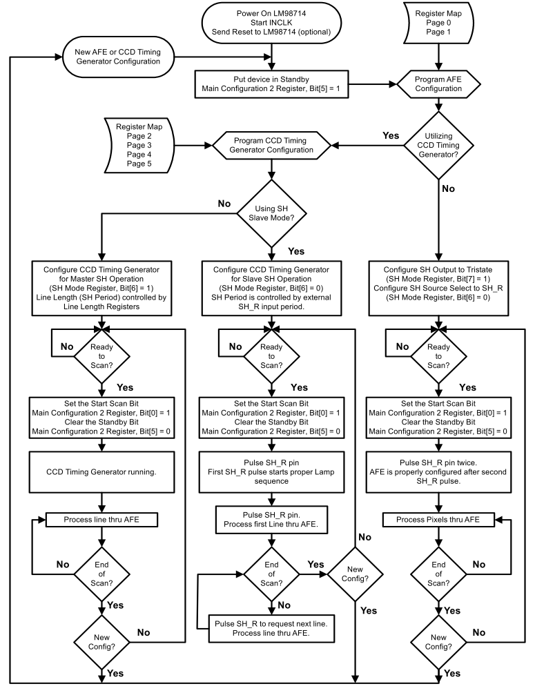 Figure 60. LM98714 Proper Sequence of Operation
Table 11. Page 0 Register Table - Main Analog Front End Configuration
| Address (Binary) | Register Title (Mnemonic) | Default (Binary) | Register/Bit Description | |||||||
|---|---|---|---|---|---|---|---|---|---|---|
| Bit 7 | Bit 6 | Bit 5 | Bit 4 | Bit 3 | Bit 2 | Bit 1 | Bit 0 | |||
| Note: The active register page is selected by writing the desired value to the page select register 1Fh. This register is mirrored on all register pages. | ||||||||||
| Page 0 | Page Register 1F = 0000 0000 | |||||||||
| 00000 | Main Configuration 0 | 1111 0001 | Operating Mode Select | |||||||
| 00001 | Main Configuration 1 | 0101 0000 | Source Follower Enable | Input Bias Enable | Input Polarity | Sampling Mode Select | Output Format | PIXCLK/ ADCCLK Config. | Pixel Phase Clock Select | |
| 00010 | Main Configuration 2 | 0000 0000 | Not Used | Active/ Standby | Gain Mode Select | Output Enable | Power-down | Soft Reset | Start Scan | |
| 00011 | Main Configuration 3 | 0000 0111 | Processing Channel Override | Reserved | ||||||
| 00100 | Main Configuration 4 | 0000 0000 | Not Used | Upcount Enable | LVDS Test Mode | |||||
| 00101 | Input Clamp Control | 0000 0000 | Not Used | Auto CLPIN Width | Auto CLPIN Enable | CLPIN Gating | ||||
| 00110 | Auto CLPIN Position | 0010 0111 | MSB | LSB | ||||||
| 00111 | VCLP Configuration | 0010 0000 | Not Used | VCLP Reference Select | VCLP DAC Bits | |||||
| 01000 | Black Level Clamp Control | 0000 0000 | Line Averaging | Pixel Averaging | Offset Integration | BLKCLP Mode Select | ||||
| 01001 | Auto Black Level Clamp Position | 0000 0000 | Not Used | MSB | LSB | |||||
| 01010 | Target Black Level MSB | 0010 0000 | MSB | LSB+2 | ||||||
| 01011 | Target Black Level LSB | 0000 0000 | Not Used | LSB+1 | LSB | |||||
| 01100 | OSR CLAMP Control | 0000 0000 | Not Used | CLAMPR Position | ||||||
| 01101 | OSG CLAMP Control | 0000 0000 | Not Used | CLAMPG Position | ||||||
| 01110 | OSB CLAMP Control | 0000 0000 | Not Used | CLAMPB Position | ||||||
| 01111 | OSR SAMPLE Control | 0000 0000 | Not Used | SAMPLER Position | ||||||
| 10000 | OSG SAMPLE Control | 0000 0000 | Not Used | SAMPLEG Position | ||||||
| 10001 | OSB SAMPLE Control | 0000 0000 | Not Used | SAMPLEB Position | ||||||
| 10010 | Upcounter Register 1 | 0000 0000 | Count Value LSBs | |||||||
| 10011 | Upcounter Register 2 | 0000 0000 | Count Value Middle 8 Bits | |||||||
| 10100 | Upcounter Register 3 | 0000 0000 | Not Used | Count Value MSBs | ||||||
| 10101 | ||||||||||
| 10110 | ||||||||||
| 10111 | ||||||||||
| 11000 | ||||||||||
| 11001 | ||||||||||
| 11010 | ||||||||||
| 11011 | ||||||||||
| 11100 | ||||||||||
| 11101 | ||||||||||
| 11110 | 0000 0100 | |||||||||
| 11111 | Page Register | 0000 0000 | Reserved (program all zeros) | LSB+2 | LSB+1 | LSB | ||||
Table 12. Page 1 Register Table - Offset and Gain Settings
| Address (Binary) | Register Title (Mnemonic) | Default (Binary) | Register/Bit Description | |||||||
|---|---|---|---|---|---|---|---|---|---|---|
| Bit 7 | Bit 6 | Bit 5 | Bit 4 | Bit 3 | Bit 2 | Bit 1 | Bit 0 | |||
| Note: The active register page is selected by writing the desired value to the page select register 1Fh. This register is mirrored on all register pages. | ||||||||||
| Page 1 | Page Register 1F = 0000 0001 | |||||||||
| 00000 | Color 1 PGA | 0101 0100 | MSB | LSB | ||||||
| 00001 | Color 2 PGA | 0101 0100 | MSB | LSB | ||||||
| 00010 | Color 3 PGA | 0101 0100 | MSB | LSB | ||||||
| 00011 | Color 4 PGA | 0101 0100 | MSB | LSB | ||||||
| 00100 | Color 5 PGA | 0101 0100 | MSB | LSB | ||||||
| 00101 | Color 1 Black Level Offset DAC MSB | 1000 0000 | MSB | LSB+2 | ||||||
| 00110 | Color 1 Black Level Offset DAC LSB | 0000 0000 | Not Used | LSB+1 | LSB | |||||
| 00111 | Color 2 Black Level Offset DAC MSB | 1000 0000 | MSB | LSB+2 | ||||||
| 01000 | Color 2 Black Level Offset DAC LSB | 0000 0000 | Not Used | LSB+1 | LSB | |||||
| 01001 | Color 3 Black Level Offset DAC MSB | 1000 0000 | MSB | LSB+2 | ||||||
| 01010 | Color 3 Black Level Offset DAC LSB | 0000 0000 | Not Used | LSB+1 | LSB | |||||
| 01011 | Color 4 Black Level Offset DAC MSB | 1000 0000 | MSB | LSB+2 | ||||||
| 01100 | Color 4 Black Level Offset DAC LSB | 0000 0000 | Not Used | LSB+1 | LSB | |||||
| 01101 | Color 5 Black Level Offset DAC MSB | 1000 0000 | MSB | LSB+2 | ||||||
| 01110 | Color 5 Black Level Offset DAC LSB | 0000 0000 | Not Used | LSB+1 | LSB | |||||
| 01111 | Color 1 Digital Offset | 0100 0000 | Not Used | MSB | LSB | |||||
| 10000 | Color 2 Digital Offset | 0100 0000 | Not Used | MSB | LSB | |||||
| 10001 | Color 3 Digital Offset | 0100 0000 | Not Used | MSB | LSB | |||||
| 10010 | Color 4 Digital Offset | 0100 0000 | Not Used | MSB | LSB | |||||
| 10011 | Color 5 Digital Offset | 0100 0000 | Not Used | MSB | LSB | |||||
| 10100 | ||||||||||
| 10101 | ||||||||||
| 10110 | ||||||||||
| 10111 | ||||||||||
| 11000 | ||||||||||
| 11001 | ||||||||||
| 11010 | ||||||||||
| 11011 | ||||||||||
| 11100 | ||||||||||
| 11101 | ||||||||||
| 11110 | 0000 0100 | |||||||||
| 11111 | Page Register | 0000 0000 | Reserved (program all zeros) | LSB+2 | LSB+1 | LSB | ||||
Table 13. Page 2 Register Table - CCD/CIS Timing Generator Control 1
| Address (Binary) | RegisterTitle (Mnemonic) | Default (Binary) | Register/Bit Description | |||||||
|---|---|---|---|---|---|---|---|---|---|---|
| Bit 7 | Bit 6 | Bit 5 | Bit 4 | Bit 3 | Bit 2 | Bit 1 | Bit 0 | |||
| Note: The active register page is selected by writing the desired value to the page select register 1Fh. This register is mirrored on all register pages. | ||||||||||
| Page 2 | Page Register 1F = 0000 0010 | |||||||||
| 00000 | SH Mode | 0000 0000 | SH Output Enable | SH Source Select | SH Mode | SH Delay | ||||
| 00001 | SH Pulse Width | 0010 0111 | SH Pulse Width | |||||||
| 00010 | PIX1/2 Control | 1100 1000 | PIX1 Activity | PIX1 Polarity | PIX1 Frequency | PIX1 Activity During SH | PIX2 Activity | PIX2 Polarity | PIX2 Frequency | PIX2 Activity During SH |
| 00011 | PIX3/4 Control | 1000 1000 | PIX3 Activity | PIX3 Polarity | PIX3 Frequency | PIX3 Activity During SH | PIX4 Activity | PIX4 Polarity | PIX4 Frequency | PIX4 Activity During SH |
| 00100 | PIX5/6 Control | 0000 0000 | PIX5 Activity | PIX5 Polarity | PIX5 Frequency | PIX5 Activity During SH | PIX6 Activity | PIX6 Polarity | PIX6 Frequency | PIX6 Activity During SH |
| 00101 | PIX7/8 Control | 0000 0000 | PIX7 Activity | PIX7 Polarity | PIX7 Frequency | PIX7 Activity During SH | PIX8 Activity | PIX8 Polarity | PIX8 Frequency | PIX8 Activity During SH |
| 00110 | Line Clamp Enable | 0000 0000 | PIX8 Line Clamp Enable | PIX7 Line Clamp Enable | PIX6 Line Clamp Enable | PIX5 Line Clamp Enable | PIX4 Line Clamp Enable | PIX3 Line Clamp Enable | PIX2 Line Clamp Enable | PIX1 Line Clamp Enable |
| 00111 | PIX1 Start | 0000 0000 | Reserved | MSB | LSB | |||||
| 01000 | PIX1 End | 0001 0101 | Reserved | MSB | LSB | |||||
| 01001 | ||||||||||
| 01010 | PIX2 Start | 0000 0000 | Reserved | MSB | LSB | |||||
| 01011 | PIX2 End | 0001 0101 | Reserved | MSB | LSB | |||||
| 01100 | ||||||||||
| 01101 | PIX3 Start | 0000 1011 | Reserved | MSB | LSB | |||||
| 01110 | PIX3 End | 0000 1101 | Reserved | MSB | LSB | |||||
| 01111 | ||||||||||
| 10000 | PIX4 Start | 0001 0000 | Reserved | MSB | LSB | |||||
| 10001 | PIX4 End | 0001 0011 | Reserved | MSB | LSB | |||||
| 10010 | ||||||||||
| 10011 | PIX5 Start | 0000 0000 | Reserved | MSB | LSB | |||||
| 10100 | PIX5 End | 0000 0000 | Reserved | MSB | LSB | |||||
| 10101 | ||||||||||
| 10110 | PIX6 Start | 0000 0000 | Reserved | MSB | LSB | |||||
| 10111 | PIX6 End | 0000 0000 | Reserved | MSB | LSB | |||||
| 11000 | ||||||||||
| 11001 | PIX7 Start | 0000 0000 | Reserved | MSB | LSB | |||||
| 11010 | PIX7 End | 0000 0000 | Reserved | MSB | LSB | |||||
| 11011 | ||||||||||
| 11100 | PIX8 Start | 0000 0000 | Reserved | MSB | LSB | |||||
| 11101 | PIX8 End | 0000 0000 | Reserved | MSB | LSB | |||||
| 11110 | CMOS Data Mode | 0000 0000 | Reserved | CLK10/ CLKOUT | CLK9/ CB[4] | CLK8/ CB[3] | CLK7/ CB[2] | CLK6/ CB[1] | CLK5/ CB[0] | |
| Status Bit Enable | ||||||||||
| 11111 | Page Register | 0000 0000 | Reserved (program all zeros) | LSB+2 | LSB+1 | LSB | ||||
Table 14. Page 3 Register Table - CCD/CIS Timing Generator Control 2
| Address (Binary) | Register Title (Mnemonic) | Default (Binary) | Register/Bit Description | |||||||
|---|---|---|---|---|---|---|---|---|---|---|
| Bit 7 | Bit 6 | Bit 5 | Bit 4 | Bit 3 | Bit 2 | Bit 1 | Bit 0 | |||
| Note: The active register page is selected by writing the desired value to the page select register 1Fh. This register is mirrored on all register pages. | ||||||||||
| Page 3 | Page Register 1F = 0000 0011 | |||||||||
| 00000 | Output Mapping CLK1/CLK2 |
0000 0000 | Output Mapping for CLK1 Pin | Output Mapping for CLK2 Pin | ||||||
| 00001 | Output Mapping CLK3/CLK4 |
0000 0000 | Output Mapping for CLK3 Pin | Output Mapping for CLK4 Pin | ||||||
| 00010 | Output Mapping CLK5/CLK6 |
0000 0000 | Output Mapping for CLK5 Pin | Output Mapping for CLK6 Pin | ||||||
| 00011 | Output Mapping CLK7/CLK8 |
0000 0000 | Output Mapping for CLK7 Pin | Output Mapping for CLK9 Pin | ||||||
| 00100 | Output Mapping CLK9/(CLKOUT/ CLK10) |
0000 0000 | Output Mapping for CLK9 Pin | Output Mapping for CLKOUT/CLK10 Pin | ||||||
| 00101 | Illumination Mode | 0000 0000 | LAMPR
Normal State |
LAMPG
Normal State |
LAMPB
Normal State |
LampIR1 Normal State |
LampIR2 Normal State |
Reserved | SH/LAMP Overlap Enable |
|
| 00110 | Line 1 Lamp Selection | 0000 0000 | Red Lamp Enable | Green Lamp Enable | Blue Lamp Enable | IR1 Lamp Enable | IR2 Lamp Enable | |||
| 00111 | Line 2 Lamp Selection | 0000 0000 | Red Lamp Enable | Green Lamp Enable | Blue Lamp Enable | IR1 Lamp Enable | IR2 Lamp Enable | |||
| 01000 | Line 3 Lamp Selection | 0000 0000 | Red Lamp Enable | Green Lamp Enable | Blue Lamp Enable | IR1 Lamp Enable | IR2 Lamp Enable | |||
| 01001 | Line 4 Lamp Selection | 0000 0000 | Red Lamp Enable | Green Lamp Enable | Blue Lamp Enable | IR1 Lamp Enable | IR2 Lamp Enable | |||
| 01010 | Line 5 Lamp Selection | 0000 0000 | Red Lamp Enable | Green Lamp Enable | Blue Lamp Enable | IR1 Lamp Enable | IR2 Lamp Enable | |||
| 01011 | LAMPR On - MSB | 0000 0000 | Reserved | SH_OR Enable | MSB | |||||
| 01100 | LAMPR On - LSB | 0001 0001 | LSB | |||||||
| 01101 | LAMPR Off - MSB | 0000 0011 | Reserved | MSB | ||||||
| 01110 | LAMPR Off - LSB | 0000 0110 | LSB | |||||||
| 01111 | LAMPG On - MSB | 0000 0000 | Reserved | SH_OR Enable | MSB | |||||
| 010000 | LAMPG On - LSB | 0001 0010 | LSB | |||||||
| 10001 | LAMPG Off - MSB | 0000 0011 | Reserved | MSB | ||||||
| 10010 | LAMPG Off - LSB | 0000 0000 | LSB | |||||||
| 10011 | LAMPB On - MSB | 0000 0000 | Reserved | SH_OR Enable | MSB | |||||
| 10100 | LAMPB On - LSB | 0001 0011 | LSB | |||||||
| 10101 | LAMPB Off - MSB | 0000 0011 | Reserved | MSB | ||||||
| 10110 | LAMPB Off - LSB | 0011 0000 | LSB | |||||||
| 10111 | LAMPIR1 On - MSB | 0000 0000 | Reserved | SH_OR Enable | MSB | |||||
| 11000 | LAMPIR1 On - LSB | 0001 0100 | LSB | |||||||
| 11001 | LAMPIR1 Off - MSB | 0000 0011 | Reserved | MSB | ||||||
| 11010 | LAMPIR1 Off - LSB | 0011 0000 | LSB | |||||||
| 11011 | LAMPIR2 On - MSB | 0000 0000 | Reserved | SH_OR Enable | MSB | |||||
| 11100 | LAMPIR2 On - LSB | 0001 0101 | LSB | |||||||
| 11101 | LAMPIR2 Off - MSB | 0000 0011 | Reserved | MSB | ||||||
| 11110 | LAMPIR2 Off - LSB | 0011 0000 | LSB | |||||||
| 11111 | Page Register | 0000 0000 | Reserved (program all zeros) | LSB+2 | LSB+1 | LSB | ||||
Table 15. Page 4 Register Table - CCD/CIS Timing Generator Control 3
| Address (Binary) | Register Title (Mnemonic) | Default (Binary) | Register/Bit Description | |||||||
|---|---|---|---|---|---|---|---|---|---|---|
| Bit 7 | Bit 6 | Bit 5 | Bit 4 | Bit 3 | Bit 2 | Bit 1 | Bit 0 | |||
| Note: The active register page is selected by writing the desired value to the page select register 1Fh. This register is mirrored on all register pages. | ||||||||||
| Page 4 | Page Register 1F = 0000 0100 | |||||||||
| 00000 | Mode On - MSB | 0000 0010 | Reserved | MSB | ||||||
| 00001 | Mode On - LSB | 0000 0000 | LSB | |||||||
| 00010 | Mode Off - MSB | 0000 0011 | Reserved | MSB | ||||||
| 00011 | Mode Off - LSB | 0000 0001 | LSB | |||||||
| 00100 | Optical Black Pixels Start | 0000 0000 | MSB | LSB | ||||||
| 00101 | Optical Black Pixels End | 0000 0000 | MSB | LSB | ||||||
| 00110 | Start of Valid Pixels - MSB | 0000 0000 | Reserved | MSB | ||||||
| 00111 | Start of Valid Pixels - LSB | 0000 0001 | LSB | |||||||
| 01000 | End of Valid Pixels - MSB | 0011 1111 | Reserved | MSB | ||||||
| 01001 | End of Valid Pixels - LSB | 1111 1110 | LSB | |||||||
| 01010 | Line End - MSB | 0011 1111 | Reserved | MSB | ||||||
| 01011 | Line End - LSB | 1111 1111 | LSB | |||||||
| 01100 | Sample Timing Monitor 1 | 1111 1111 | ||||||||
| 01101 | Sample Timing Monitor 2 | 1111 1111 | ||||||||
| 01110 | Sample Timing Monitor 3 | 1111 1111 | ||||||||
| 01111 | SH2/SH3 Control | 0000 0000 | SH3 Select | SH2 Select | ||||||
| 10000 | PIX OR/NOR Control 1 | 0000 0000 | ||||||||
| 10001 | PIX OR/NOR Control 2 | 0000 0000 | ||||||||
| 11111 | Page Register | 0000 0000 | Reserved (program all zeros) | LSB+2 | LSB+1 | LSB | ||||
Table 16. Page 5 Register Table - CCD/CIS Timing Generator Control 4
| Address (Binary) | Register Title (Mnemonic) | Default (Binary) | Register/Bit Description | |||||||
|---|---|---|---|---|---|---|---|---|---|---|
| Bit 7 | Bit 6 | Bit 5 | Bit 4 | Bit 3 | Bit 2 | Bit 1 | Bit 0 | |||
| Note: The active register page is selected by writing the desired value to the page select register 1Fh. This register is mirrored on all register pages. | ||||||||||
| Page 5 | Page Register 1F = 0000 0101 | |||||||||
| 00000 | PIX1/SH On Guardbands | 0000 1111 | PIX1 On Guardband | |||||||
| 00001 | PIX1/SH Off Guardbands | 0000 0111 | PIX1 Off Guardband | |||||||
| 00010 | PIX2/SH On Guardbands | 0000 1111 | PIX2 On Guardband | |||||||
| 00011 | PIX2/SH Off Guardbands | 0000 0111 | PIX2 Off Guardband | |||||||
| 00100 | PIX3/SH On Guardbands | 0000 1111 | PIX3 On Guardband | |||||||
| 00101 | PIX3/SH Off Guardbands | 0000 0111 | PIX3 Off Guardband | |||||||
| 00110 | PIX4/SH On Guardbands | 0000 1111 | PIX4 On Guardband | |||||||
| 00111 | PIX4/SH Off Guardbands | 0000 0111 | PIX4 Off Guardband | |||||||
| 01000 | PIX5/SH On Guardbands | 0000 1111 | PIX5 On Guardband | |||||||
| 01001 | PIX5/SH Off Guardbands | 0000 0111 | PIX5 Off Guardband | |||||||
| 01010 | PIX6/SH On Guardbands | 0000 1111 | PIX6 On Guardband | |||||||
| 01011 | PIX6/SH Off Guardbands | 0000 0111 | PIX6 Off Guardband | |||||||
| 01100 | PIX7/SH On Guardbands | 0000 1111 | PIX7 On Guardband | |||||||
| 01101 | PIX7/SH Off Guardbands | 0000 0111 | PIX7 Off Guardband | |||||||
| 01110 | PIX8/SH On Guardbands | 0000 1111 | PIX8 On Guardband | |||||||
| 01111 | PIX8/SH Off Guardbands | 0000 0111 | PIX8 Off Guardband | |||||||
| 11111 | Page Register | 0000 0000 | Reserved (program all zeros) | LSB+2 | LSB+1 | LSB | ||||
7.6.2 Register Definition
Table 17. Register Descriptions
| Page | Address (Binary) |
Register Title |
Default (Binary) |
Bit No. | Description |
|---|---|---|---|---|---|
| Page 0 Registers | |||||
| 0 | 0 0000 | Main Configuration 0 | 1111 0001 | [7:0] | Main Configuration Register 0 |
| [7:6] | Mode Select Bits. | ||||
| 11 Mode 3 (Default) (3 Channel Mode) | |||||
| 10 Mode 2 (2 Channel Mode) | |||||
| 01 Mode 1a (1 Channel Mode, 1 Channel sampled for all lines) | |||||
| 00 Mode 1b (3 Channel Line rate mode, 1 Channel sampled per line) | |||||
| [5:4] | Color Select Bits. Used to determine the inputs sampled during a scan. | ||||
| 11 All three channels sampled (Default) | |||||
| 10 Mode 2 = OSR & OSB Mode 1 = OSB | |||||
| 01 Mode 2 = OSG & OSB Mode 1 = OSG | |||||
| 00 Mode 2 = OSR & OSG Mode 1 = OSR | |||||
| [3] | Color Order. Configures the sequence of the pixel processing. | ||||
| 0 Forward (default) | |||||
| 1 Reverse | |||||
| [2:0] | Color Sequence Length. Used in Mode 1a only to determine the number of lines of colors sequenced during a scan. | ||||
| 111 Not valid | |||||
| 110 Not Valid | |||||
| 101 Five color (line) sequence | |||||
| 100 Four color (line) sequence | |||||
| 011 Three color (line) sequence | |||||
| 010 Two color (line) sequence | |||||
| 001 One color (line) sequence (Default) | |||||
| 000 Not Valid | |||||
| 0 | 0 0001 | Main Configuration 1 | 0101 0000 | [7:0] | Main Configuration Register 1 |
| [7] | Source Follower Enable. | ||||
| 0 Disable (Default) | |||||
| 1 Enable | |||||
| [6] | Input Bias Enable. Enables the Input Bias Resistor ladder. | ||||
| 0 Disable | |||||
| 1 Enable (Default) | |||||
| [5] | Input Polarity. Configures the polarity mode of the input signal. | ||||
| 0 Negative going input relative to reference (Default) | |||||
| 1 Positive going input relative to reference | |||||
| [4] | Sampling Mode Select. | ||||
| 0 Sample and Hold Mode | |||||
| 1 Correlated Double Sampling Mode (Default) | |||||
| [3] | Output Format. | ||||
| 0 LVDS (Default) | |||||
| 1 CMOS | |||||
| [2] | PIXCLK/ADCCLK Configuration. Selects appropriate multiplier for given input clock frequency. | ||||
| Mode 3: ADC Frequency = 3x Pixel Frequency | |||||
| Mode 2: ADC Frequency = 2x Pixel Frequency | |||||
| Mode 1: ADC Frequency = 1x Pixel Frequency | |||||
| 0 ADCCLK User supplies ADC rate clock, LM98714 performs no multiplication | |||||
| 1 PIXCLK User supplies Pixel rate clock, LM98714 performs clock multiplication | |||||
| Mode 3: PIXCLK internally multiplied by 3 to get ADC clock | |||||
| Mode 2: PIXCLK internally multiplied by 2 to get ADC clock | |||||
| Mode 1: PIXCLK = ADCCLK. This bit is not used for Mode 1 | |||||
| [1:0] | Pixel Phase Clock Select. Coarse adjustment for Pixel phase relative to INCLK. Useful in systems where Pixel inputs arrive with significant delay relative to INCLK. | ||||
| 00 PIXPHASE0. Pixel phase aligned with INCLK | |||||
| 01 PIXPHASE1. Pixel phase delayed by (TADC Clock* 3/7) | |||||
| 10 PIXPHASE2. Pixel phase delayed by (TADC Clock) | |||||
| 11 PIXPHASE3. Pixel phase delayed by (TADC Clock * (1 + 3/7)) | |||||
| 0 | 0 0010 | Main Configuration 2 | 0000 0000 | [7:0] | Main Configuration 2 |
| [7:6] | Not Used | ||||
| [5] | Active/Standby | ||||
| [4] | Gain Mode Select. Selects either a 1x or 2x gain mode in the CDS/Sample/Hold Block. | ||||
| 0 1x Gain in the CDS/Sample/Hold Block (Default) | |||||
| 1 2x Gain in the CDS/Sample/Hold Block | |||||
| [3] | Output Enable. Enables the Data Output pins. | ||||
| 0 Disabled (Default) | |||||
| 1 Enable | |||||
| [2] | Powerdown | ||||
| 0 Device fully powered (Default) | |||||
| 1 Powerdown. Power down of major analog blocks | |||||
| [1] | Software Reset. Performs a system reset when set to a 1. Self clearing. | ||||
| [0] | Start Scan (BOS) | ||||
| 0 Ready (Default) | |||||
| 1 Start Scan. Control bit is self clearing | |||||
| 0 | 0 0011 | Main Configuration 3 | 0000 0111 | [7:0] | Main Configuration 3 |
| [7:4] | Not Used | ||||
| [3] | Processing Channel Override. Used in Mode 1 to determine the analog processing path for the selected inputs. | ||||
| 0 Multiplex all selected inputs into the Red Channel analog path (Default) | |||||
| 1 Process each selected input through its respective analog path | |||||
| [2:0] | Reserved Set to 111 |
||||
| 0 | 0 0100 | Main Configuration 4 | 0000 0000 | [7:0] | Main Configuration 4 |
| [7:4] | Not Used | ||||
| [3] | Upcount Enable | ||||
| [2:0] | LVDS Test Mode. Activates LVDS test pattern output (when in LVDS output mode only). | ||||
| 000 Normal operation, no test pattern output (Default) | |||||
| 001 Test pattern 1: Alternating pattern between 0x155555 and 0x0AAAAA | |||||
| 010 Test pattern 2: If Upcount Enable Bit set, count from 21h000000 to 21h 1FFFFF | |||||
| 011 Test pattern 3. Output Static Count value found represented by the three Upcounter Registers found on page 0 | |||||
| Reg 0x14 Bits[4:0] = Count Values 5 MSBs | |||||
| Reg 0x13 Bits[7:0] = Count Values 8 Middle Bits | |||||
| Reg 0x12 Bits[7:0] = Count Values 8 LSBs | |||||
| 0 | 0 0101 | Input Clamp Control | 0000 0000 | [7:0] | Input Clamp Control (CLPIN) Configuration Register |
| [7:4] | Reserved | ||||
| [3:2] | Auto CLPIN Width. Width in Pixels of the Auto generated CLPIN pulse. | ||||
| 00 4 Pixels (Default) | |||||
| 01 8 Pixels | |||||
| 10 16 Pixels | |||||
| 11 32 Pixels | |||||
| [1] | Auto CLPIN Enable. | ||||
| 0 Auto CLPIN Disabled | |||||
| CLPIN Pulse generation Disabled (Default) | |||||
| 1 Auto CLPIN | |||||
| CLPIN generated internally with a programmable delay from SH | |||||
| [0] | CLPIN Gating Enable. | ||||
| 0 Auto CLPINGATED not gated by SAMPLE (default) | |||||
| 1 Auto CLPINGATED gated by SAMPLE (= logical and of CLPIN and SAMPLE) | |||||
| 0 | 0 0110 | Auto CLPIN Position | 0010 0111 | [7:0] | Auto CLPIN Pulse Position Register |
| [7:0] | Auto CLPIN Pulse Position. Number of pixels in which Auto CLPIN pulse is delayed, relative to the falling edge of SH. | ||||
| 0 | 0 0111 | VCLP Configuration | 0010 0000 | [7:0] | VCLP Configuration Register |
| [7:6] | Reserved | ||||
| [5:4] | VCLP Reference Select. | ||||
| 00 External Bias (No Internal Connection to Ladder Resistors or DAC) | |||||
| 01 Internal VCLP DAC connection only | |||||
| 10 Internal Resistor Ladder connection only (Default) | |||||
| 11 Reserved | |||||
| [3:0] | 4 Bit nibble for VCLP Reference DAC value. | ||||
| 0 | 0 1000 | Black Level Clamp Control | 0000 0000 | [7:0] | Black Level Correction Circuitry Configuration Register |
| [7:6] | Line Averaging. Number of Lines that the correction loop will run. Line Counter is reset during any write to this register. A line beginning is defined by the SH pulse. | ||||
| 00 Infinite (Default) | |||||
| 01 15 Lines | |||||
| 10 31 Lines | |||||
| 11 63 Lines | |||||
| [5:4] | Pixel Averaging. Number of Black Level Pixels averaged by the correction loop. | ||||
| 00 4 Pixels | |||||
| 01 8 Pixels | |||||
| 10 16 Pixels | |||||
| 11 32 Pixels | |||||
| [3:2] | Offset Integration. | ||||
| 00 Divide by 8 | |||||
| 01 Divide by 16 | |||||
| 10 Divide by 32 | |||||
| 11 Divide by 64 | |||||
| [1:0] | BLKCLP Mode Select. If Auto Black Clamp pulse is enabled, Offset DAC registers are read only. | ||||
| 00 Auto Black Clamp Circuitry Disabled (default) | |||||
| 01 Auto Black Clamp pulse delayed from falling edge of SH pulse | |||||
| 10 Auto Black Clamp pulse delayed from falling edge of CLPIN pulse | |||||
| 11 Reserved | |||||
| 0 | 0 1001 | Auto Black Level Clamp Position | 0000 0000 | [7] | Reserved |
| [6:0] | Black Level Clamp Position. Number of pixels in which Auto Black pulse is delayed, relative to selected trigger source. | ||||
| 0 | 0 1010 | Target Black Level MSB | 0010 0000 | [7:0] | The 8 MSBs of the 10 Bit target output code for black pixels when using the Auto Black Level Correction loop. |
| 0 | 0 1011 | Target Black Level LSB | 0000 0000 | [7:0] | The target output code for black pixels when using the Auto Black Level Correction loop |
| [7:2] | Reserved | ||||
| [1:0] | The 2 LSBs of the 10 Bit target output code for black pixels when using the Auto Black Level Correction loop. | ||||
| 0 | 0 1100 | OSR CLAMP Control | 0000 0000 | [7:5] | Not Used |
| [4:0] | CLAMPR Position. A value of 0 will force the position of this pulse to be at the mode dependant default. | ||||
| 0 | 0 1101 | OSG CLAMP Control | 0000 0000 | [7:5] | Not Used |
| [4:0] | CLAMPG Position. A value of 0 will force the position of this pulse to be at the mode dependant default. | ||||
| 0 | 0 1110 | OSB CLAMP Control | 0000 0000 | [7:5] | Not Used |
| [4:0] | CLAMPB Position. A value of 0 will force the position of this pulse to be at the mode dependant default. | ||||
| 0 | 0 1111 | OS R SAMPLE Control | 0000 0000 | [7] | Not Used |
| [6:0] | SAMPLER Position. A value of 0 will force the position of this pulse to be at the mode dependant default. | ||||
| 0 | 1 0000 | OSG SAMPLE Control | 0000 0000 | [7] | Not Used |
| [6:0] | SAMPLEG Position. A value of 0 will force the position of this pulse to be at its mode dependant default. | ||||
| 0 | 1 0001 | OSB SAMPLE Control | 0000 0000 | [7] | Not Used |
| [6:0] | SAMPLEB Position. A value of 0 will force the position of this pulse to be at its mode dependant default. | ||||
| 0 | 1 1111 | Page Register | 0000 0000 | [7:0] | Used to select desired page of registers being accessed. |
| Page 1 Registers | |||||
| 1 | 0 0000 | Color 1 PGA | 0101 0100 | [7:0] | The eight bit byte selected by the 5:1 PGA MUX in Mode 1a during Color 1 lines. |
| In Mode 1b, Mode 2 or Mode 3, the register used to define the PGA setting for the OSR input. | |||||
| 1 | 0 0001 | Color 2 PGA | 0101 0100 | [7:0] | The eight bit byte selected by the 5:1 PGA MUX in Mode 1a during Color 2 lines. |
| In Mode 1b, Mode 2 or Mode 3, the register used to define the PGA setting for the OSG input. | |||||
| 1 | 0 0010 | Color 3 PGA | 0101 0100 | [7:0] | The eight bit byte selected by the 5:1 PGA MUX in Mode 1a during Color 3 lines. |
| In Mode 1b, Mode 2 or Mode 3, the register used to define the PGA setting for the OSB input. | |||||
| 1 | 0 0011 | Color 4 PGA | 0101 0100 | [7:0] | The eight bit byte selected by the 5:1 PGA MUX in Mode 1a during Color 4 lines. |
| Not used in Mode 1b, Mode 2 or Mode 3. | |||||
| 1 | 0 0100 | Color 5 PGA | 0101 0100 | [7:0] | The eight bit byte selected by the 5:1 PGA MUX in Mode 1a during Color 5 lines. |
| Not used in Mode 1b, Mode 2 or Mode 3. | |||||
| 1 | 0 0101 | Color 1 Black Level DAC MSB | 1000 0000 | [7:0] | The MSBs selected by the 5:1 DAC MUX in Mode 1a during Color 1 lines. |
| In Mode 1b/c, Mode 2 or Mode 3, the register used to define the DAC setting for the OSR input. The DAC value is in offset Binary format. | |||||
| 1 | 0 0110 | Color 1 Black Level DAC LSB | 0000 0000 | [7:0] | Color 1 Black Level DAC LSB |
| [7:2] | Not Used | ||||
| [1:0] | The LSBs selected by the 5:1 DAC MUX in Mode 1a during Color 1 lines. | ||||
| In Mode 1b, Mode 2 or Mode 3, the register used to define the DAC setting for the OSR input. The DAC value is in offset Binary format. | |||||
| 1 | 0 0111 | Color 2 Black Level DAC MSB | 1000 0000 | [7:0] | The MSBs selected by the 5:1 DAC MUX in Mode 1a during Color 2 lines. |
| In Mode 1b, Mode 2 or Mode 3, the register used to define the DAC setting for the OSG input. The DAC value is in offset Binary format. | |||||
| 1 | 0 1000 | Color 2 Black Level DAC LSB | 0000 0000 | [7:0] | Color 2 Black Level DAC LSB |
| [7:2] | Not Used | ||||
| [1:0] | The LSBs selected by the 5:1 DAC MUX in Mode 1a during Color 2 lines. | ||||
| In Mode 1b, Mode 2 or Mode 3, the register used to define the DAC setting for the OSG input. The DAC value is in offset Binary format. | |||||
| 1 | 0 1001 | Color 3 Black Level DAC MSB | 1000 0000 | [7:0] | The MSBs selected by the 5:1 DAC MUX in Mode 1a during Color 3 lines. |
| In Mode 1b, Mode 2 or Mode 3, the register used to define the DAC setting for the OSB input. The DAC value is in offset Binary format. | |||||
| 1 | 0 1010 | Color 3 Black Level DAC LSB | 0000 0000 | [7:0] | Color 3 Black Level DAC LSB |
| [7:2] | Not Used | ||||
| [1:0] | The LSBs selected by the 5:1 DAC MUX in Mode 1a during Color 3 lines. | ||||
| In Mode 1b, Mode 2 or Mode 3, the register used to define the DAC setting for the OSB input. The DAC value is in offset Binary format. | |||||
| 1 | 0 1011 | Color 4 Black Level DAC MSB | 1000 0000 | [7:0] | The MSBs selected by the 5:1 DAC MUX in Mode 1a during Color 4 lines. |
| Not used in Mode 1b, Mode 2 or Mode 3. The DAC value is in offset Binary format. | |||||
| 1 | 0 1100 | Color 4 Black Level DAC LSB | 0000 0000 | [7:0] | Color 4 Black Level DAC LSB |
| [7:2] | Not Used | ||||
| [1:0] | The LSBs selected by the 5:1 DAC MUX in Mode 1a during Color 4 lines. | ||||
| Not used in Mode 1b, Mode 2 or Mode 3. The DAC value is in offset Binary format. | |||||
| 1 | 0 1101 | Color 5 Black Level DAC MSB | 1000 0000 | [7:0] | The MSBs selected by the 5:1 DAC MUX in Mode 1a during Color 5 lines. |
| Not used in Mode 1b, Mode 2 or Mode 3. The DAC value is in offset Binary format. | |||||
| 1 | 0 1110 | Color 5 Black Level DAC LSB | 0000 0000 | [7:0] | Color 5 Black Level DAC LSB |
| [7:2] | Not Used | ||||
| [1:0] | The LSBs selected by the 5:1 DAC MUX in Mode 1a during Color 5 lines. | ||||
| Not used in Mode 1b/c, Mode 2 or Mode 3. The DAC value is in offset Binary format. | |||||
| 1 | 0 1111 | Color 1 Digital Offset | 0100 0000 | [7:0] | Color 1 Digital Offset |
| [7] | Not Used | ||||
| [6:0] | The Digital Offset applied to the ADC result in Mode 1a during Color 1 lines. | ||||
| In Mode 1b/c, Mode 2 or Mode 3, the register used to define the Digital Offset setting for the OSR input. The DAC value is in offset Binary format. | |||||
| 1 | 1 0000 | Color 2 Digital Offset | 0100 0000 | [7:0] | Color 2 Digital Offset |
| [7] | Not Used | ||||
| [6:0] | The Digital Offset applied to the ADC result in Mode 1a during Color 2 lines. | ||||
| In Mode 1b/c, Mode 2 or Mode 3, the register used to define the DAC setting for the OSG input. The DAC value is in offset Binary format. | |||||
| 1 | 1 0001 | Color 3 Digital Offset | 0100 0000 | [7:0] | Color 3 Digital Offset |
| [7] | Not Used | ||||
| [6:0] | The Digital Offset applied to the ADC result in Mode 1a during Color 3 lines. | ||||
| In Mode 1b/c, Mode 2 or Mode 3, the register used to define the DAC setting for the OSB input. The DAC value is in offset Binary format. | |||||
| 1 | 1 0010 | Color 4 Digital Offset | 0100 0000 | [7:0] | Color 4 Digital Offset |
| [7] | Not Used | ||||
| [6:0] | The Digital Offset applied to the ADC result in Mode 1a during Color 4 lines. | ||||
| Not used in Mode 1b/c, Mode 2 or Mode 3. The DAC value is in offset Binary format. | |||||
| 1 | 1 0011 | Color 5 Digital Offset | 0100 0000 | [7:0] | Color 5 Digital Offset |
| [7] | Not Used | ||||
| [6:0] | The Digital Offset applied to the ADC result in Mode 1a during Color 5 lines. | ||||
| Not used in Mode 1b/c, Mode 2 or Mode 3. The DAC value is in offset Binary format. | |||||
| 1 | 1 1111 | Page Register | 0000 0000 | [7:0] | Used to select desired page of registers being accessed. |
| Page 2 Registers | |||||
| 2 | 0 0000 | SH Mode | 0000 0000 | [7] | SH Output Enable. |
| 0 Enable SH Output | |||||
| 1 SH Output Tristate | |||||
| [6] | SH Master/Slave Select. | ||||
| 0 External SH_R input. CCD Timing Generator runs in Slave mode, with SH triggered by an external pulse on the SH_R pin. | |||||
| 1 Auto generated SH. CCD Timing Generator runs in Master mode, with SH generated internally with a programmable period and width. | |||||
| [5:4] | SH Output Mode. | ||||
| 00 SH Output = SH | |||||
| 01 SH Output = SH | |||||
| 10 SH Output = 0 | |||||
| 11 SH Output = 1 | |||||
| [3:0] | SH Delay from SH_R | ||||
| Additional delay | |||||
| 2 | 0 0001 | SH Pulse Width | 0010 0111 | [7:0] | SH Pulse Width |
| SH Pulse Width = (2 * [7:0]) + 1 | |||||
| 2 | 0 0010 | PIX1/2 Control | 1100 1000 | [7] | PIX1 Activity |
| 0 Disabled | |||||
| 1 Enabled | |||||
| [6] | PIX1 Polarity | ||||
| 0 Normal - Low when off | |||||
| 1 Inverted - High when off | |||||
| [5] | PIX1 Frequency | ||||
| 0 Pixel Rate | |||||
| 1 1/2 Pixel Rate | |||||
| [4] | PIX1 Activity During SH | ||||
| 0 Inactive | |||||
| 1 Active | |||||
| [3] | PIX2 Activity | ||||
| 0 Disabled | |||||
| 1 Enabled | |||||
| [2] | PIX2 Polarity | ||||
| 0 Normal - Low when off | |||||
| 1 Inverted - High when off | |||||
| [1] | PIX2 Frequency | ||||
| 0 Pixel Rate | |||||
| 1 1/2 Pixel Rate | |||||
| [0] | PIX2 Activity During SH | ||||
| 0 Inactive | |||||
| 1 Active | |||||
| 2 | 0 0011 | PIX3/4 Control | 1000 1000 | [7] | PIX3 Activity |
| 0 Disabled | |||||
| 1 Enabled | |||||
| [6] | PIX3 Polarity | ||||
| 0 Normal - Low when off | |||||
| 1 Inverted - High when off | |||||
| [5] | PIX3 Frequency | ||||
| 0 Pixel Rate | |||||
| 1 1/2 Pixel Rate | |||||
| [4] | PIX3 Activity During SH | ||||
| 0 Inactive | |||||
| 1 Active | |||||
| [3] | PIX4 Activity | ||||
| 0 Disabled | |||||
| 1 Enabled | |||||
| [2] | PIX4 Polarity | ||||
| 0 Normal - Low when off | |||||
| 1 Inverted - High when off | |||||
| [1] | PIX4 Frequency | ||||
| 0 Pixel Rate | |||||
| 1 1/2 Pixel Rate | |||||
| [0] | PIX4 Activity During SH | ||||
| 0 Inactive | |||||
| 1 Active | |||||
| 2 | 0 0100 | PIX5/6 Control | 0000 0000 | [7] | PIX5 Activity |
| 0 Disabled | |||||
| 1 Enabled | |||||
| [6] | PIX5 Polarity | ||||
| 0 Normal - Low when off | |||||
| 1 Inverted - High when off | |||||
| [5] | PIX5 Frequency | ||||
| 0 Pixel Rate | |||||
| 1 1/2 Pixel Rate | |||||
| [4] | PIX5 Activity During SH | ||||
| 0 Inactive | |||||
| 1 Active | |||||
| [3] | PIX6 Activity | ||||
| 0 Disabled | |||||
| 1 Enabled | |||||
| [2] | PIX6 Polarity | ||||
| 0 Normal - Low when off. | |||||
| 1 Inverted - High when off. | |||||
| [1] | PIX6 Frequency | ||||
| 0 Pixel Rate | |||||
| 1 1/2 Pixel Rate | |||||
| [0] | PIX6 Activity During SH | ||||
| 0 Inactive | |||||
| 1 Active | |||||
| 2 | 0 0101 | PIX7/8 Control | 0000 0000 | [7] | PIX7 Activity |
| 0 Disabled | |||||
| 1 Enabled | |||||
| [6] | PIX7 Polarity | ||||
| 0 Normal - Low when off | |||||
| 1 Inverted - High when off | |||||
| [5] | PIX7 Frequency | ||||
| 0 Pixel Rate | |||||
| 1 1/2 Pixel Rate | |||||
| [4] | PIX7 Activity During SH | ||||
| 0 Inactive | |||||
| 1 Active | |||||
| [3] | PIX8 Activity | ||||
| 0 Disabled | |||||
| 1 Enabled | |||||
| [2] | PIX8 Polarity | ||||
| 0 Normal - Low when off | |||||
| 1 Inverted - High when off | |||||
| [1] | PIX8 Frequency | ||||
| 0 Pixel Rate | |||||
| 1 1/2 Pixel Rate | |||||
| [0] | PIX8 Activity During SH | ||||
| 0 Inactive | |||||
| 1 Active | |||||
| 2 | 0 0110 | Line Clamp Enable | 0000 0000 | [7] | PIX8 Line Clamp Enable. Enables single Line Clamp pulse per line from PIX8. |
| 0 Disabled. PIX generator functions as normal. | |||||
| 1 Enabled. PIX generates a single clock per line for Line Clamp function. | |||||
| [6] | PIX7 Line Clamp Enable. Enables single Line Clamp pulse per line from PIX7. | ||||
| 0 Disabled. PIX generator functions as normal. | |||||
| 1 Enabled. PIX generates a single clock per line for Line Clamp function. | |||||
| [5] | PIX6 Line Clamp Enable. Enables single Line Clamp pulse per line from PIX6. | ||||
| 0 Disabled. PIX generator functions as normal. | |||||
| 1 Enabled. PIX generates a single clock per line for Line Clamp function. | |||||
| [4] | PIX5 Line Clamp Enable. Enables single Line Clamp pulse per line from PIX5. | ||||
| 0 Disabled. PIX generator functions as normal. | |||||
| 1 Enabled. PIX generates a single clock per line for Line Clamp function. | |||||
| PIX4 Line Clamp Enable. Enables single Line Clamp pulse per line from PIX4. | |||||
| [3] | 0 Disabled. PIX generator functions as normal. | ||||
| 1 Enabled. PIX generates a single clock per line for Line Clamp function. | |||||
| PIX3 Line Clamp Enable. Enables single Line Clamp pulse per line from PIX3. | |||||
| [2] | 0 Disabled. PIX generator functions as normal. | ||||
| 1 Enabled. PIX generates a single clock per line for Line Clamp function. | |||||
| PIX2 Line Clamp Enable. Enables single Line Clamp pulse per line from PIX2. | |||||
| [1] | 0 Disabled. PIX generator functions as normal. | ||||
| 1 Enabled. PIX generates a single clock per line for Line Clamp function. | |||||
| PIX1 Line Clamp Enable. Enables single Line Clamp pulse per line from PIX1. | |||||
| [0] | 0 Disabled. PIX generator functions as normal. | ||||
| 1 Enabled. PIX generates a single clock per line for Line Clamp function. | |||||
| 2 | 0 0111 | PIX1 Start | 0000 0000 | [7] | Reserved. Set to 0. |
| [6:0] | PIX1 on point. Defines when the PIX1 signal turns on within the pixel period. Can be set to any available edge within the pixel period. (For 1/2 frequency signals, the count can be any available edge within 2 pixel periods) | ||||
| 2 | 0 1000 | PIX1 End | 0001 0101 | [7] | Reserved. Set to 0. |
| [6:0] | PIX1 off point. Defines when the PIX1 signal turns off within the pixel period. Can be set to any available edge within the pixel period. (For 1/2 frequency signals, the count can be any available edge within 2 pixel periods) | ||||
| 2 | 0 1010 | PIX2 Start | 0000 0000 | [7] | Reserved. Set to 0. |
| [6:0] | PIX2 on point. Defines when the PIX2 signal turns on within the pixel period. Can be set to any available edge within the pixel period. (For 1/2 frequency signals, the count can be any available edge within 2 pixel periods) | ||||
| 2 | 0 1011 | PIX2 End | 0001 0101 | [7] | Reserved. Set to 0. |
| [6:0] | PIX2 off point. Defines when the PIX2 signal turns off within the pixel period. Can be set to any available edge within the pixel period. (For 1/2 frequency signals, the count can be any available edge within 2 pixel periods) | ||||
| 2 | 0 1101 | PIX3 Start | 0000 1011 | [7] | Reserved. Set to 0. |
| [6:0] | PIX3 on point. Defines when the PIX3 signal turns on within the pixel period. Can be set to any available edge within the pixel period. (For 1/2 frequency signals, the count can be any available edge within 2 pixel periods) | ||||
| 2 | 0 1110 | PIX3 End | 0000 1101 | [7] | Reserved. Set to 0. |
| [6:0] | PIX3 off point. Defines when the PIX3 signal turns off within the pixel period. Can be set to any available edge within the pixel period. (For 1/2 frequency signals, the count can be any available edge within 2 pixel periods) | ||||
| 2 | 1 0000 | PIX4 Start | 0001 0000 | [7] | Reserved. Set to 0. |
| [6:0] | PIX4 on point. Defines when the PIX4 signal turns on within the pixel period. Can be set to any available edge within the pixel period. (For 1/2 frequency signals, the count can be any available edge within 2 pixel periods) | ||||
| 2 | 1 0001 | PIX4 End | 0001 0011 | [7] | Reserved. Set to 0. |
| [6:0] | PIX4 off point. Defines when the PIX4 signal turns off within the pixel period. Can be set to any available edge within the pixel period. (For 1/2 frequency signals, the count can be any available edge within 2 pixel periods) | ||||
| 2 | 1 0011 | PIX5 Start | 0000 0000 | [7] | Reserved. Set to 0. |
| [6:0] | PIX5 on point. Defines when the PIX5 signal turns on within the pixel period. Can be set to any available edge within the pixel period. (For 1/2 frequency signals, the count can be any available edge within 2 pixel periods) | ||||
| 2 | 1 0100 | PIX5 End | 0000 0000 | [7] | Reserved. Set to 0. |
| [6:0] | PIX5 off point. Defines when the PIX5 signal turns off within the pixel period. Can be set to any available edge within the pixel period. (For 1/2 frequency signals, the count can be any available edge within 2 pixel periods) | ||||
| 2 | 1 0110 | PIX6 Start | 0000 0000 | [7] | Reserved. Set to 0. |
| [6:0] | PIX6 on point. Defines when the PIX6 signal turns on within the pixel period. Can be set to any available edge within the pixel period. (For 1/2 frequency signals, the count can be any available edge within 2 pixel periods) | ||||
| 2 | 1 0111 | PIX6 End | 0000 0000 | [7] | Reserved. Set to 0. |
| [6:0] | PIX6 off point. Defines when the PIX6 signal turns off within the pixel period. Can be set to any available edge within the pixel period. (For 1/2 frequency signals, the count can be any available edge within 2 pixel periods) | ||||
| 2 | 1 1001 | PIX7 Start | 0000 0000 | [7] | Reserved. Set to 0. |
| [6:0] | PIX7 on point. Defines when the PIX7 signal turns on within the pixel period. Can be set to any available edge within the pixel period. (For 1/2 frequency signals, the count can be any available edge within 2 pixel periods) | ||||
| 2 | 1 1010 | PIX7 End | 0000 0000 | [7] | Reserved. Set to 0. |
| [6:0] | PIX7 off point. Defines when the PIX7 signal turns off within the pixel period. Can be set to any available edge within the pixel period. (For 1/2 frequency signals, the count can be any available edge within 2 pixel periods) | ||||
| 2 | 1 1100 | PIX8 Start | 0000 0000 | [7] | Reserved. Set to 0. |
| [6:0] | PIX8 on point. Defines when the PIX8 signal turns on within the pixel period. Can be set to any available edge within the pixel period. (For 1/2 frequency signals, the count can be any available edge within 2 pixel periods) | ||||
| 2 | 1 1101 | PIX8 End | 0000 0000 | [7] | Reserved. Set to 0 |
| [6:0] | PIX8 off point. Defines when the PIX8 signal turns off within the pixel period. Can be set to any available edge within the pixel period. (For 1/2 frequency signals, the count can be any available edge within 2 pixel periods) | ||||
| 2 | 1 1110 | CMOS Data Mode Status Bit Enable | 0000 0000 | [7:6] | Reserved. Set to 000 |
| When mapping the CLK5 to CLK10 pins as either CLKOUT or CB outputs, the Sample Timing Monitor 1 (Page 4, Register 0x0C) cannot be used. | |||||
| [5] | 0 - CLK10 mapped normally, 1- CLK10 = CLKOUT | ||||
| [4] | 0 - CLK9 mapped normally, 1- CLK9 = CB[4] status bit | ||||
| [3] | 0 - CLK8 mapped normally, 1- CLK8 = CB[3] status bit | ||||
| [2] | 0 - CLK7 mapped normally, 1- CLK7 = CB[2] status bit | ||||
| [1] | 0 - CLK6 mapped normally, 1- CLK6 = CB[1] status bit | ||||
| [0] | 0 - CLK5 mapped normally, 1- CLK5 = CB[0] status bit | ||||
| 2 | 1 1111 | Page Register | 0000 0000 | [7:0] | Used to select desired page of registers being accessed. |
| Page 3 Registers | |||||
| 3 | 0 0000 | Output Mapping CLK1/CLK2 This register sets which timing signal is present on the respective CLKn output pin. |
0000 0000 | [7:4] CLK 1 |
Setting CLKn = |
| 0000 Tristate | |||||
| 0001 PIX1 | |||||
| 0010 PIX2 | |||||
| 0011 PIX3 | |||||
| 0100 PIX4 | |||||
| 0101 PIX5 | |||||
| 0110 PIX6 | |||||
| 0111 PIX7 | |||||
| [3:0] CLK 2 |
1000 PIX8 | ||||
| 1001 LAMPR | |||||
| 1010 LAMPG | |||||
| 1011 LAMPB | |||||
| 1100 LAMPIR1 | |||||
| 1101 LAMPIR2 | |||||
| 1110 MODE | |||||
| 1111 SH | |||||
| 3 | 0 0001 | Output Mapping CLK3/CLK4 This register sets which timing signal is present on the respective CLKn output pin. |
0000 0000 | [7:4] CLK 3 |
Setting CLKn = |
| 0000 Tristate | |||||
| 0001 PIX1 | |||||
| 0010 PIX2 | |||||
| 0011 PIX3 | |||||
| 0100 PIX4 | |||||
| 0101 PIX5 | |||||
| 0110 PIX6 | |||||
| 0111 PIX7 | |||||
| [3:0] CLK 4 |
1000 PIX8 | ||||
| 1001 LAMPR | |||||
| 1010 LAMPG | |||||
| 1011 LAMPB | |||||
| 1100 LAMPIR1 | |||||
| 1101 LAMPIR2 | |||||
| 1110 MODE | |||||
| 1111 SH | |||||
| 3 | 0 0010 | Output Mapping CLK5/CLK6 This register sets which timing signal is present on the respective CLKn output pin. |
0000 0000 | [7:0] CLK 5 |
Setting CLKn = |
| 0000 Tristate | |||||
| 0001 PIX1 | |||||
| 0010 PIX2 | |||||
| 0011 PIX3 | |||||
| 0100 PIX4 | |||||
| 0101 PIX5 | |||||
| 0110 PIX6 | |||||
| 0111 PIX7 | |||||
| [3:0] CLK 6 |
1000 PIX8 | ||||
| 1001 LAMPR | |||||
| 1010 LAMPG | |||||
| 1011 LAMPB | |||||
| 1100 LAMPIR1 | |||||
| 1101 LAMPIR2 | |||||
| 1110 MODE | |||||
| 1111 SH | |||||
| 3 | 0 0011 | Output Mapping CLK7/CLK8 This register sets which timing signal is present on the respective CLKn output pin. |
0000 0000 | [7:0] CLK 7 |
Setting CLKn = |
| 0000 Tristate | |||||
| 0001 PIX1 | |||||
| 0010 PIX2 | |||||
| 0011 PIX3 | |||||
| 0100 PIX4 | |||||
| 0101 PIX5 | |||||
| 0110 PIX6 | |||||
| 0111 PIX7 | |||||
| [3:0] CLK 8 |
1000 PIX8 | ||||
| 1001 LAMPR | |||||
| 1010 LAMPG | |||||
| 1011 LAMPB | |||||
| 1100 LAMPIR1 | |||||
| 1101 LAMPIR2 | |||||
| 1110 MODE | |||||
| 1111 SH | |||||
| 3 | 0 0100 | Output Mapping CLK9/CLK10 This register sets which timing signal is present on the respective CLKn output pin. |
0000 0000 | [7:4] CLK 9 |
Setting CLKn = |
| 0000 Tristate | |||||
| 0001 PIX1 | |||||
| 0010 PIX2 | |||||
| 0011 PIX3 | |||||
| 0100 PIX4 | |||||
| 0101 PIX5 | |||||
| 0110 PIX6 | |||||
| 0111 PIX7 | |||||
| [3:0] CLK 10 |
1000 PIX8 | ||||
| 1001 LAMPR | |||||
| 1010 LAMPG | |||||
| 1011 LAMPB | |||||
| 1100 LAMPIR1 | |||||
| 1101 LAMPIR2 | |||||
| 1110 MODE | |||||
| 1111 SH | |||||
| 3 | 0 0101 | Illumination Mode (see also AFE color modes) | 0000 0000 | [7] | LAMPR Normal State |
| 0 = Low, 1 = High | |||||
| [6] | LAMPG Normal State | ||||
| 0 = Low, 1 = High | |||||
| [5] | LAMPB Normal State | ||||
| 0 = Low, 1 = High | |||||
| [4] | LampIR1 Normal State | ||||
| 0 = Low, 1 = High | |||||
| [3] | LampIR2 Normal State | ||||
| 0 = Low, 1 = High | |||||
| [2:1] | Reserved | ||||
| [0] | SH/LAMP Overlap Enable | ||||
| 0 Disabled | |||||
| 1 Overlap Enabled | |||||
| 3 | 0 0110 | Line 1 Lamp Selection | 0000 0000 | [7:5] | Reserved. Set to 000 |
| [4] | Red Lamp Enable | ||||
| 0 Red Disabled | |||||
| 1 Red Enabled | |||||
| [3] | Green Lamp Enable | ||||
| 0 Green Disabled | |||||
| 1 Green Enabled | |||||
| [2] | Blue Lamp Enable | ||||
| 0 Blue Disabled | |||||
| 1 Blue Enabled | |||||
| [1] | IR1 Lamp Enable | ||||
| 0 IR1 Disabled | |||||
| 1 IR1 Enabled | |||||
| [0] | IR2 Lamp Enable | ||||
| 0 IR2 Disabled | |||||
| 1 IR2 Enabled | |||||
| 3 | 0 0111 | Line 2 Lamp Selection | 0000 0000 | [7:5] | Reserved. Set to 000 |
| [4] | Red Lamp Enable | ||||
| 0 Red Disabled | |||||
| 1 Red Enabled | |||||
| [3] | Green Lamp Enable | ||||
| 0 Green Disabled | |||||
| 1 Green Enabled | |||||
| [2] | Blue Lamp Enable | ||||
| 0 Blue Disabled | |||||
| 1 Blue Enabled | |||||
| [1] | IR1 Lamp Enable | ||||
| 0 IR1 Disabled | |||||
| 1 IR1 Enabled | |||||
| [0] | IR2 Lamp Enable | ||||
| 0 IR2 Disabled | |||||
| 1 IR2 Enabled | |||||
| 3 | 0 1000 | Line 3 Lamp Selection | 0000 0000 | [7:5] | Reserved. Set to 000 |
| [4] | Red Lamp Enable | ||||
| 0 Red Disabled | |||||
| 1 Red Enabled | |||||
| [3] | Green Lamp Enable | ||||
| 0 Green Disabled | |||||
| 1 Green Enabled | |||||
| [2] | Blue Lamp Enable | ||||
| 0 Blue Disabled | |||||
| 1 Blue Enabled | |||||
| [1] | IR1 Lamp Enable | ||||
| 0 IR1 Disabled | |||||
| 1 IR1 Enabled | |||||
| [0] | IR2 Lamp Enable | ||||
| 0 IR2 Disabled | |||||
| 1 IR2 Enabled | |||||
| 3 | 0 1001 | Line 4 Lamp Selection | 0000 0000 | [7:5] | Reserved. Set to 000 |
| [4] | Red Lamp Enable | ||||
| 0 Red Disabled | |||||
| 1 Red Enabled | |||||
| [3] | Green Lamp Enable | ||||
| 0 Green Disabled | |||||
| 1 Green Enabled | |||||
| [2] | Blue Lamp Enable | ||||
| 0 Blue Disabled | |||||
| 1 Blue Enabled | |||||
| [1] | IR1 Lamp Enable | ||||
| 0 IR1 Disabled | |||||
| 1 IR1 Enabled | |||||
| [0] | IR2 Lamp Enable | ||||
| 0 IR2 Disabled | |||||
| 1 IR2 Enabled | |||||
| 3 | 0 1010 | Line 5 Lamp Selection | 0000 0000 | [7:5] | Reserved. Set to 000 |
| [4] | Red Lamp Enable | ||||
| 0 Red Disabled | |||||
| 1 Red Enabled | |||||
| [3] | Green Lamp Enable | ||||
| 0 Green Disabled | |||||
| 1 Green Enabled | |||||
| [2] | Blue Lamp Enable | ||||
| 0 Blue Disabled | |||||
| 1 Blue Enabled | |||||
| [1] | IR1 Lamp Enable | ||||
| 0 IR1 Disabled | |||||
| 1 IR1 Enabled | |||||
| [0] | IR2 Lamp Enable | ||||
| 0 IR2 Disabled | |||||
| 1 IR2 Enabled | |||||
| 3 | 0 1011 | LAMPR On MSB | 0000 0000 | [7:5] | Reserved. Set to 000 |
| [4] | LAMPR SH_OR Enable | ||||
| 0 No ORing | |||||
| 1 LAMPR uses SH_OR function | |||||
| [3:0] | LAMPR On Time Most Significant Bits | ||||
| This selects the pixel count at which the LAMPR output goes high. | |||||
| 3 | 0 1100 | LAMPR On LSB | 0001 0001 | [7:0] | LAMPR On Time Least Significant Byte |
| This selects the pixel count at which the LAMPR output goes high. | |||||
| 3 | 0 1101 | LAMPR Off MSB | 0000 0011 | [7:4] | Reserved. Set to 0000 |
| [3:0] | LAMPR Off Time Most Significant Bits | ||||
| This selects the pixel count at which the LAMPR output goes low. | |||||
| 3 | 0 1110 | LAMPR Off LSB | 0000 0110 | [7:0] | LAMPR Off Time Least Significant Byte |
| This selects the pixel count at which the LAMPR output goes low. | |||||
| 3 | 0 1111 | LAMPG On MSB | 0000 0000 | [7:5] | Reserved. Set to 000 |
| [4] | LAMPG SH_OR Enable. | ||||
| 0 No ORing | |||||
| 1 LAMPG uses SH_OR function | |||||
| [3:0] | LAMPG On Time Most Significant Bits. | ||||
| This selects the pixel count at which the LAMPR output goes high. | |||||
| 3 | 1 0000 | LAMPG On LSB | 0001 0010 | [7:0] | LAMPG On Time Least Significant Byte |
| This selects the pixel count at which the LAMPR output goes high. | |||||
| 3 | 1 0001 | LAMPG Off MSB | 0000 0011 | [7:4] | Reserved. Set to 0000 |
| [3:0] | LAMPG Off Time Most Significant Bits | ||||
| This selects the pixel count at which the LAMPR output goes low. | |||||
| 3 | 1 0010 | LAMPG Off LSB | 0000 0000 | [7:0] | LAMPG Off Time Least Significant Byte |
| This selects the pixel count at which the LAMPR output goes low. | |||||
| 3 | 1 0011 | LAMPB On MSB | 0000 0000 | [7:5] | Reserved. Set to 000 |
| [4] | LAMPB SH_OR Enable | ||||
| 0 No ORing | |||||
| 1 LAMPB uses SH_OR function | |||||
| [3:0] | LAMPB On Time Most Significant Bits | ||||
| This selects the pixel count at which the LAMPR output goes high. | |||||
| 3 | 1 0100 | LAMPB On LSB | 0001 0011 | [7:0] | LAMPB On Time Least Significant Byte |
| This selects the pixel count at which the LAMPR output goes high. | |||||
| 3 | 1 0101 | LAMPB Off MSB | 0000 0011 | [7:4] | Reserved. Set to 0000 |
| [3:0] | LAMPB Off Time Most Significant Bits | ||||
| This selects the pixel count at which the LAMPR output goes low. | |||||
| 3 | 1 0110 | LAMPB Off LSB | 0011 0000 | [7:0] | LAMPB Off Time Least Significant Byte |
| This selects the pixel count at which the LAMPR output goes low. | |||||
| 3 | 1 0111 | LAMPIR1 On MSB | 0000 0000 | [7:5] | Reserved. Set to 000 |
| [4] | LAMPIR1 SH_OR Enable | ||||
| 0 No ORing | |||||
| 1 LAMPIR1 uses SH_OR function | |||||
| [3:0] | LAMPIR1 On Time Most Significant Bits | ||||
| This selects the pixel count at which the LAMPR output goes high. | |||||
| 3 | 1 1000 | LAMPIR1 On LSB | 0001 0100 | [7:0] | LAMPIR1 On Time Least Significant Byte |
| This selects the pixel count at which the LAMPR output goes high. | |||||
| 3 | 1 1001 | LAMPIR1 Off MSB | 0000 0011 | [7:4] | Reserved. Set to 0000 |
| [3:0] | LAMPIR1 Off Time Most Significant Bits | ||||
| This selects the pixel count at which the LAMPR output goes low. | |||||
| 3 | 1 1010 | LAMPIR1 Off LSB | 0011 0000 | [7:0] | LAMPIR1 Off Time Least Significant Byte |
| This selects the pixel count at which the LAMPR output goes low. | |||||
| 3 | 1 1011 | LAMPIR2 On MSB | 0000 0000 | [7:5] | Reserved. Set to 000 |
| [4] | LAMPIR2 SH_OR Enable. | ||||
| 0 No ORing | |||||
| 1 LAMPIR2 uses SH_OR function | |||||
| [3:0] | LAMPIR2 On Time Most Significant Bits. | ||||
| This selects the pixel count at which the LAMPR output goes high. | |||||
| 3 | 1 1100 | LAMPIR2 On LSB | 0001 0101 | [7:0] | LAMPIR2 On Time Least Significant Byte |
| This selects the pixel count at which the LAMPR output goes high. | |||||
| 3 | 1 1101 | LAMPIR2 Off MSB | 0000 0011 | [7:4] | Reserved. Set to 0000 |
| [3:0] | LAMPIR2 Off Time Most Significant Bits | ||||
| This selects the pixel count at which the LAMPR output goes low. | |||||
| 3 | 1 1110 | LAMPIR2 Off LSB | 0011 0000 | [7:0] | LAMPIR2 Off Time Least Significant Byte |
| This selects the pixel count at which the LAMPR output goes low. | |||||
| 3 | 1 1111 | Page Register | 0000 0000 | [7:0] | Used to select desired page of registers being accessed. |
| Page 4 Registers | |||||
| 4 | 0 0000 | Mode On MSB | 0000 0010 | [7:4] | Reserved. Set to 0000 |
| [3:0] | Mode On Time Most Significant Bits | ||||
| This selects the pixel count at which the Mode output goes high. | |||||
| 4 | 0 0001 | Mode On LSB | 0000 0000 | [7:0] | Mode On Time Least Significant Byte |
| This selects the pixel count at which the Mode output goes high. | |||||
| 4 | 0 0010 | Mode Off MSB | 0000 0011 | [7:4] | Reserved. Set to 0000 |
| [3:0] | Mode Off Time Most Significant Bits | ||||
| This selects the pixel count at which the Mode output goes low. | |||||
| 4 | 0 0011 | Mode Off LSB | 0000 0001 | [7:0] | Mode Off Time Least Significant Byte |
| This selects the pixel count at which the Mode output goes low. | |||||
| 4 | 0 0100 | Optical Black Pixels Start | 0000 0000 | [7:0] | Starting point for optical black clamping |
| nnnnnnnn - n pixels (0-255) | |||||
| 4 | 0 0101 | Optical Black Pixels End | 0000 0000 | [7:0] | End point for optical black clamping |
| nnnnnnnn - n pixels (0-255) | |||||
| 4 | 0 0110 | Start of Valid Pixels - MSB | 0000 0000 | [7:6] | Reserved. Set to 00 |
| [5:0] | Start of Valid Pixels - Most Significant Bits. | ||||
| Selects the pixel count where the data status bits begin to indicate valid pixels. | |||||
| 4 | 0 0111 | Start of Valid Pixels - LSB | 0000 0000 | [7:0] | Start of Valid Pixels - Least Significant Bits. |
| Selects the pixel count where the data status bits begin to indicate valid pixels. | |||||
| 4 | 0 1000 | End of Valid Pixels - MSB | 0011 1111 | [7:6] | Reserved. Set to 00 |
| [5:0] | End of Valid Pixels - Most Significant Bits. | ||||
| Selects the pixel count where the data status bits stop indicating valid pixels. | |||||
| 4 | 0 1001 | End of Valid Pixels - LSB | 1111 1110 | [7:0] | End of Valid Pixels - Least Significant Bits. |
| Selects the pixel count where the data status bits stop indicating valid pixels. | |||||
| 4 | 0 1010 | Line End - MSB | 0011 1111 | [7:6] | Reserved. Set to 00. |
| [5:0] | Line End Value - Most Significant 6 Bits | ||||
| Selects the pixel count where the current line is ended and the next one begins. Controls the integration time of one line and the period between SH pulses. | |||||
| 4 | 0 1011 | Line End - LSB | 1111 1111 | [7:0] | Line End Value Least Significant Byte |
| Selects the pixel count where the current line is ended and the next one begins. Controls the integration time of one line and the period between SH pulses. | |||||
| n pixels (0 - 16383) | |||||
| 4 | 0 1100 | Sample Timing Monitor 1 | 1111 1111 | [7:0] | Enables Sample and Clamp timing signals to be observed on one of the sensor timing control outputs. This function overrides any other settings for sensor control signal mapping. |
| Important Note: Sample Timing Monitor 1 cannot be used if the CMOS Data Mode Status Bit Enable Register (Page 2, Register 0x1E) is being programmed to map CLKOUT to CLK10 or any Control Bit to CLK5-CLK9. Sample Timing Monitors 2 and 3 are not effected by this limitation. | |||||
| [7:4] | Upper 4 bits select timing signal to be monitored. | ||||
| 0000 Sample Red | |||||
| 0001 Clamp Red | |||||
| 0010 Sample Green | |||||
| 0011 Clamp Green | |||||
| 0100 Sample Blue | |||||
| 0101 Clamp Blue | |||||
| 1111 No signal monitored | |||||
| [3:0] | Lower 4 bits select which output pin is used as a monitor. | ||||
| 0000 CLK1 | |||||
| 0001 CLK2 | |||||
| 0010 CLK3 | |||||
| 0011 CLK4 | |||||
| 0100 CLK5 | |||||
| 0101 CLK6 | |||||
| 0110 CLK7 | |||||
| 0111 CLK8 | |||||
| 1000 CLK9 | |||||
| 1001 CLKOUT/CLK10 | |||||
| 1111 All outputs normal | |||||
| 4 | 0 1101 | Sample Timing Monitor 2 | 1111 1111 | [7:0] | Enables Sample and Clamp timing signals to be observed on one of the sensor timing control outputs. This function overrides any other settings for sensor control signal mapping. |
| [7:4] | Upper 4 bits select timing signal to be monitored. | ||||
| 0000 Sample Red | |||||
| 0001 Clamp Red | |||||
| 0010 Sample Green | |||||
| 0011 Clamp Green | |||||
| 0100 Sample Blue | |||||
| 0101 Clamp Blue | |||||
| 1111 No signal monitored | |||||
| [3:0] | Lower 4 bits select which output pin is used as a monitor. | ||||
| 0000 CLK1 | |||||
| 0001 CLK2 | |||||
| 0010 CLK3 | |||||
| 0011 CLK4 | |||||
| 0100 CLK5 | |||||
| 0101 CLK6 | |||||
| 0110 CLK7 | |||||
| 0111 CLK8 | |||||
| 1000 CLK9 | |||||
| 1001 CLKOUT/CLK10 | |||||
| 1111 All outputs normal | |||||
| 4 | 0 1110 | Sample Timing Monitor 3 | 1111 1111 | [7:0] | Enables Sample and Clamp timing signals to be observed on one of the sensor timing control outputs. This function overrides any other settings for sensor control signal mapping. |
| [7:4] | Upper 4 bits select timing signal to be monitored. | ||||
| 0000 Sample Red | |||||
| 0001 Clamp Red | |||||
| 0010 Sample Green | |||||
| 0011 Clamp Green | |||||
| 0100 Sample Blue | |||||
| 0101 Clamp Blue | |||||
| 1111 No signal monitored | |||||
| [3:0] | Lower 4 bits select which output pin is used as a monitor. | ||||
| 0000 CLK1 | |||||
| 0001 CLK2 | |||||
| 0010 CLK3 | |||||
| 0011 CLK4 | |||||
| 0100 CLK5 | |||||
| 0101 CLK6 | |||||
| 0110 CLK7 | |||||
| 0111 CLK8 | |||||
| 1000 CLK9 | |||||
| 1001 CLKOUT/CLK10 | |||||
| 1111 All outputs normal | |||||
| 4 | 0 1111 | SH2/SH3 Control | 0000 0000 | [7:0] | Controls the optional SH2 and SH3 output signals. These signals can override the Lamp IR1 and Lamp IR2 outputs if additional SH signals are required. |
| [7:4] | Not Used. | ||||
| [3] | SH3 Output Select. | ||||
| 0 Lamp IR2 output is programmed from Lamp IR2 Generator | |||||
| 1 Lamp IR2 output is SH3 | |||||
| [2] | SH2 Output Select. | ||||
| 0 Lamp IR1 output is programmed from Lamp IR1 Generator | |||||
| 1 Lamp IR1 output is SH2 | |||||
| [1:0] | Not Used | ||||
| 4 | 1 0000 | PIX OR/NOR Control 1 | 0000 0000 | [7:0] | Controls the optional OR and NOR operations on the PIX generator outputs as described below. These signals can override the normal PIX generator outputs to pro vide OR and NOR functionality for uses such as Pixel Lumping. If multiple functions are selected, the order of priority from highest to lowest is PIX OR/NOR Control 1 Bit[0] to Bit [7], then PIX OR/NOR Control 2 Bit[0] to Bit[7] (i.e PIX OR/NOR Control 1 Bit[7] has a higher priority on the PIX5 output than PIX OR/NOR Control 2 Bit[0] or Bit[2]). |
| For reference purposes, the normal, unmodified PIX generator outputs are named pix1 through pix8 (lower case) and the final signal prior to the CLK pins are named PIX1 through PIX8 (upper case). | |||||
| [0] | 0 No effect (default); 1 PIX1 = ~(pix1 || pix2) | ||||
| [1] | 0 No effect (default); 1 PIX2 = (pix1 || pix2) | ||||
| [2] | 0 No effect (default); 1 PIX2 = ~(pix2 || pix3) | ||||
| [3] | 0 No effect (default); 1 PIX3 = (pix2 || pix3) | ||||
| [4] | 0 No effect (default); 1 PIX3 = ~(pix3 || pix4) | ||||
| [5] | 0 No effect (default); 1 PIX4 = (pix3 || pix4) | ||||
| [6] | 0 No effect (default); 1 PIX4 = ~(pix4 || pix5) | ||||
| [7] | 0 No effect (default); 1 PIX5 = (pix4 || pix5) | ||||
| 4 | 1 0001 | PIX OR/NOR Control 2 | 0000 0000 | [7:0] | Controls the optional OR and NOR operations on the PIX generator outputs as described below. These signals can override the normal PIX generator outputs to pro vide OR and NOR functionality for uses such as Pixel Lumping. If multiple functions are selected, the order of priority from highest to lowest is PIX OR/NOR Control 1 Bit[0] to Bit [7], then PIX OR/NOR Control 2 Bit[0] to Bit[7] (i.e PIX OR/NOR Control 1 Bit[7] has a higher priority on the PIX5 output than PIX OR/NOR Control 2 Bit[0] or Bit[2]). |
| For reference purposes, the normal, unmodified PIX generator outputs are named pix1 through pix8 (lower case) and the final signal prior to the CLK pins are named PIX1 through PIX8 (upper case). | |||||
| [0] | 0 No effect (default); 1 PIX5 = ~(pix5 || pix6) | ||||
| [1] | 0 No effect (default); 1 PIX6 = (pix5 || pix6) | ||||
| [2] | 0 No effect (default); 1 PIX5 = ~(pix4 || pix5 || pix6) | ||||
| [3] | 0 No effect (default); 1 PIX6 = (pix4 || pix5 || pix6) | ||||
| [4] | 0 No effect (default); 1 PIX7 = ~(pix3 || pix7 || pix8) | ||||
| [5] | 0 No effect (default); 1 PIX8 = (pix3 || pix7 || pix8) | ||||
| [6] | 0 No effect (default); 1 PIX7 = ~(pix7 || pix8) | ||||
| [7] | 0 No effect (default); 1 PIX8 = (pix7 || pix8) | ||||
| 4 | 1 1111 | Page Register | 0000 0000 | [7:0] | Used to select desired page of registers being accessed. |
| Page 5 Registers | |||||
| 5 | 0 0000 | PIX1/SH On Guardbands | 0000 1111 | [7:0] | PIX1 on guardband. Number of pixel periods from end of SH pulse to start of PIX1. |
| 5 | 0 0001 | PIX1/SH Off Guardbands | 0000 0111 | [7:0] | PIX1 off guardband. Number of pixel periods before start of SH pulse that PIX1 stops. |
| 5 | 0 0010 | PIX2/SH On Guardbands | 0000 1111 | [7:0] | PIX2 on guardband. Number of pixel periods from end of SH pulse to start of PIX2. |
| 5 | 0 0011 | PIX2/SH Off Guardbands | 0000 0111 | [7:0] | PIX2 off guardband. Number of pixel periods before start of SH pulse that PIX2 stops. |
| 5 | 0 0100 | PIX3/SH On Guardbands | 0000 1111 | [7:0] | PIX3 on guardband. Number of pixel periods from end of SH pulse to start of PIX3. |
| 5 | 0 0101 | PIX3/SH Off Guardbands | 0000 0111 | [7:0] | PIX3 off guardband. Number of pixel periods before start of SH pulse that PIX3 stops. |
| 5 | 0 0110 | PIX4/SH On Guardbands | 0000 1111 | [7:0] | PIX4 on guardband. Number of pixel periods from end of SH pulse to start of PIX4. |
| 5 | 0 0111 | PIX4/SH Off Guardbands | 0000 0111 | [7:0] | PIX4 off guardband. Number of pixel periods before start of SH pulse that PIX4 stops. |
| 5 | 0 1000 | PIX5/SH On Guardbands | 0000 1111 | [7:0] | PIX5 on guardband. Number of pixel periods from end of SH pulse to start of PIX5. |
| 5 | 0 1001 | PIX5/SH Off Guardbands | 0000 0111 | [7:0] | PIX5 off guardband. Number of pixel periods before start of SH pulse that PIX5 stops. |
| 5 | 0 1010 | PIX6/SH On Guardbands | 0000 1111 | [7:0] | PIX6 on guardband. Number of pixel periods from end of SH pulse to start of PIX6. |
| 5 | 0 1011 | PIX6/SH Off Guardbands | 0000 0111 | [7:0] | PIX6 off guardband. Number of pixel periods before start of SH pulse that PIX6 stops. |
| 5 | 0 1100 | PIX7/SH On Guardbands | 0000 1111 | [7:0] | PIX7 on guardband. Number of pixel periods from end of SH pulse to start of PIX7. |
| 5 | 0 1101 | PIX7/SH Off Guardbands | 0000 0111 | [7:0] | PIX7 off guardband. Number of pixel periods before start of SH pulse that PIX7 stops. |
| 5 | 0 1110 | PIX8/SH On Guardbands | 0000 1111 | [7:0] | PIX8 on guardband. Number of pixel periods from end of SH pulse to start of PIX8. |
| 5 | 0 1111 | PIX8/SH Off Guardbands | 0000 0111 | [7:0] | PIX8 off guardband. Number of pixel periods before start of SH pulse that PIX8 stops. |