SNOS469J April 2000 – January 2015 LM8261
PRODUCTION DATA.
9 Layout
9.1 Layout Guidelines
Generally, a good high frequency layout will keep power supply and ground traces away from the inverting input and output pins. Parasitic capacitances on these nodes to ground will cause frequency response peaking and possible circuit oscillations. Texas Instruments suggests the following evaluation boards as a guide for high frequency layout and as an aid in device testing and characterization. See Table 2 for details. The LM8261 evaluation board(s) is a good example of high frequency layout techniques as a reference. General high-speed, signal-path layout suggestions include:
- Continuous ground planes are preferred for signal routing with matched impedance traces for longer runs. However, open up both ground and power planes around the capacitive sensitive input and output device pins as shown in Figure 58. After the signal is sent into a resistor, parasitic capacitance becomes more of a bandlimiting issue and less of a stability issue.
- Use good, high-frequency decoupling capacitors (0.1 μF) on the ground plane at the device power pins as shown in Figure 58. Higher value capacitors (2.2 μF) are required, but may be placed further from the device power pins and shared among devices. For best high-frequency decoupling, consider X2Y supply-decoupling capacitors that offer a much higher self-resonance frequency over standard capacitors.
- When using differential signal routing over any appreciable distance, use microstrip layout techniques with matched impedance traces.
- The input summing junction is very sensitive to parasitic capacitance. Connect any Rf, and Rg elements into the summing junction with minimal trace length to the device pin side of the resistor, as shown in Figure 59. The other side of these elements can have more trace length if needed to the source or to ground.
9.2 Layout Example
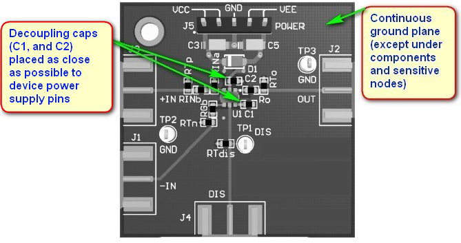 Figure 58. LM8261 Evaluation Board Layer 1
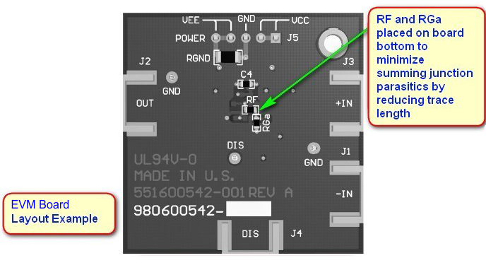 Figure 59. LM8261 Evaluation Board Layer 2
Table 2. Evaluation Board Comparison
| DEVICE | PACKAGE | EVALUATION BOARD PART NUMBER | ||
|---|---|---|---|---|
| LM8261M5 | SOT-23 | LMH730216 | ||