ZHCSLY9A October 2020 – December 2020 LM7310
PRODUCTION DATA
- 1 特性
- 2 应用
- 3 说明
- 4 Revision History
- 5 Pin Configuration and Functions
- 6 Specifications
-
7 Detailed Description
- 7.1 Overview
- 7.2 Functional Block Diagram
- 7.3
Feature Description
- 7.3.1 Input Reverse Polarity Protection
- 7.3.2 Undervoltage Protection (UVLO & UVP)
- 7.3.3 Overvoltage Lockout (OVLO)
- 7.3.4 Inrush Current control and Fast-trip
- 7.3.5 Analog Load Current Monitor Output
- 7.3.6 Reverse Current Protection
- 7.3.7 Overtemperature Protection (OTP)
- 7.3.8 Fault Response
- 7.3.9 Power Good Indication (PG)
- 7.4 Device Functional Modes
- 8 Application and Implementation
- 9 Power Supply Recommendations
- 10Layout
- 11Device and Documentation Support
- 12Mechanical, Packaging, and Orderable Information
7.3.4.1 Slew Rate (dVdt) and Inrush Current Control
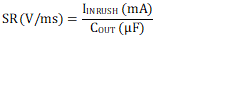
During hot-plug events or while trying to charge a large output capacitance at start-up, there can be a large inrush current. If the inrush current is not managed properly, it can damage the input connectors and/or cause the system power supply to droop leading to unexpected restarts elsewhere in the system. The inrush current during turn on is directly proportional to the load capacitance and rising slew rate. Equation 3 can be used to find the slew rate (SR) required to limit the inrush current (IINRUSH) for a given load capacitance (COUT):
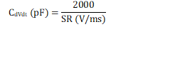
A capacitor can be connected to the dVdt pin to control the rising slew rate and lower the inrush current during turn on. The required CdVdt capacitance to produce a given slew rate can be calculated using the following equation:
The fastest output slew rate is achieved by leaving the dVdt pin open.
For CdVdt > 10 nF, it's recommended to add a 100-Ω resistor in series with the capacitor on the dVdt pin.