ZHCSLD0B May   2020  – June 2021 LM62435-Q1

PRODUCTION DATA  

  1. 特性
  2. 应用
  3. 说明
  4. Revision History
  5. Device Comparison Table
  6. Pin Configuration and Functions
  7. Specifications
    1. 7.1 Absolute Maximum Ratings
    2. 7.2 ESD Ratings
    3. 7.3 Recommended Operating Conditions
    4. 7.4 Thermal Information
    5. 7.5 Electrical Characteristics
    6. 7.6 计时特性
    7. 7.7 Systems Characteristics
    8. 7.8 Typical Characteristics
  8. Detailed Description
    1. 8.1 Overview
    2. 8.2 Functional Block Diagram
    3. 8.3 Feature Description
      1. 8.3.1  EN Uses for Enable and VIN UVLO
      2. 8.3.2  MODE/SYNC Pin Operation
        1. 8.3.2.1 Level-Dependent MODE/SYNC Pin Control
        2. 8.3.2.2 Pulse-Dependent MODE/SYNC Pin Control
        3. 8.3.2.3 Clock Locking
      3. 8.3.3  PGOOD Output Operation
      4. 8.3.4  Internal LDO, VCC UVLO, and BIAS Input
      5. 8.3.5  Bootstrap Voltage and VCBOOT-UVLO (CBOOT Pin)
      6. 8.3.6  Adjustable SW Node Slew Rate
      7. 8.3.7  Spread Spectrum
      8. 8.3.8  Soft Start and Recovery From Dropout
      9. 8.3.9  Output Voltage Setting
      10. 8.3.10 Overcurrent and Short Circuit Protection
      11. 8.3.11 Thermal Shutdown
      12. 8.3.12 Input Supply Current
    4. 8.4 Device Functional Modes
      1. 8.4.1 Shutdown Mode
      2. 8.4.2 Standby Mode
      3. 8.4.3 Active Mode
        1. 8.4.3.1 CCM Mode
        2. 8.4.3.2 Auto Mode - Light Load Operation
          1. 8.4.3.2.1 Diode Emulation
          2. 8.4.3.2.2 Frequency Reduction
        3. 8.4.3.3 FPWM Mode - Light Load Operation
        4. 8.4.3.4 Minimum On-time (High Input Voltage) Operation
        5. 8.4.3.5 Dropout
  9. Application and Implementation
    1. 9.1 Application Information
    2. 9.2 Typical Application
      1. 9.2.1 Design Requirements
      2. 9.2.2 Detailed Design Procedure
        1. 9.2.2.1  Choosing the Switching Frequency
        2. 9.2.2.2  Setting the Output Voltage
        3. 9.2.2.3  Inductor Selection
        4. 9.2.2.4  Output Capacitor Selection
        5. 9.2.2.5  Input Capacitor Selection
        6. 9.2.2.6  BOOT Capacitor
        7. 9.2.2.7  BOOT Resistor
        8. 9.2.2.8  VCC
        9. 9.2.2.9  BIAS
        10. 9.2.2.10 CFF and RFF Selection
        11. 9.2.2.11 External UVLO
      3. 9.2.3 Application Curves
  10. 10Power Supply Recommendations
  11. 11Layout
    1. 11.1 Layout Guidelines
      1. 11.1.1 Ground and Thermal Considerations
    2. 11.2 Layout Example
  12. 12Device and Documentation Support
    1. 12.1 Documentation Support
      1. 12.1.1 Related Documentation
    2. 12.2 接收文档更新通知
    3. 12.3 支持资源
    4. 12.4 Trademarks
    5. 12.5 静电放电警告
    6. 12.6 术语表
  13. 13Mechanical, Packaging, and Orderable Information

封装选项

机械数据 (封装 | 引脚)
散热焊盘机械数据 (封装 | 引脚)
订购信息

FPWM Mode - Light Load Operation

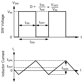
In FPWM Mode, frequency is maintained while lightly loaded. To maintain frequency, a limited reverse current is allowed to flow through the inductor. Reverse current is limited by reverse current limit circuitry, see Section 7.5 for reverse current limit values.
GUID-87B0C361-4D86-4CC6-87AA-23C0E496E04A-low.gif
In FPWM mode, Continuous Conduction (CCM) is possible even if IOUT is less than half of Iripple.
Figure 8-24 FPWM Mode Operation

Transitions between auto mode and FPWM mode can be commanded during operation if you are using the LM62435-Q1. These transitions are gradual, taking tens of clock cycles, allowing minimal disruption of output voltage during transitions. If the load is heavy enough to operate in CCM, since operation is identical in FPWM and Auto mode, no change in behavior is visible until the next time the circuit is lightly loaded.

For all devices, in FPWM mode, frequency reduction is still available if output voltage is high enough to command minimum on-time even while lightly loaded, allowing good behavior during faults which involve output being pulled up.