ZHCSLD0B May 2020 – June 2021 LM62435-Q1
PRODUCTION DATA
- 1 特性
- 2 应用
- 3 说明
- 4 Revision History
- 5 Device Comparison Table
- 6 Pin Configuration and Functions
- 7 Specifications
-
8 Detailed Description
- 8.1 Overview
- 8.2 Functional Block Diagram
- 8.3
Feature Description
- 8.3.1 EN Uses for Enable and VIN UVLO
- 8.3.2 MODE/SYNC Pin Operation
- 8.3.3 PGOOD Output Operation
- 8.3.4 Internal LDO, VCC UVLO, and BIAS Input
- 8.3.5 Bootstrap Voltage and VCBOOT-UVLO (CBOOT Pin)
- 8.3.6 Adjustable SW Node Slew Rate
- 8.3.7 Spread Spectrum
- 8.3.8 Soft Start and Recovery From Dropout
- 8.3.9 Output Voltage Setting
- 8.3.10 Overcurrent and Short Circuit Protection
- 8.3.11 Thermal Shutdown
- 8.3.12 Input Supply Current
- 8.4 Device Functional Modes
- 9 Application and Implementation
- 10Power Supply Recommendations
- 11Layout
- 12Device and Documentation Support
- 13Mechanical, Packaging, and Orderable Information
9.2.2.1 Choosing the Switching Frequency
The choice of switching frequency is a compromise between conversion efficiency and overall solution size. Lower switching frequency implies reduced switching losses and usually results in higher system efficiency. However, higher switching frequency allows for the use of smaller inductors and output capacitors, hence, a more compact design.
When choosing operating frequency, the most important consideration is thermal limitations. This constraint typically dominates frequency selection. See Figure 9-2 for circuits running at 400 kHz and Figure 9-3 for circuits running at 2.1 MHz. These curves show how much output current can be supported at a given ambient temperature given these switching frequencies. Note that power dissipation is layout-dependent so while these curves are a good starting point, thermal resistance in any design will be different from the estimates used to generate Figure 9-2 and Figure 9-3. The maximum temperature ratings are based on a 100-mm x 80-mm, 4-layer EVM PCB design, LM61460EVM.

| fSW = 400 kHz | PCB RθJA = 25°C/W | VOUT = 5 V |

| fSW = 2100 kHz | PCB RθJA = 25°C/W | VOUT = 5 V |
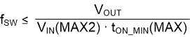
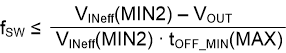
Two other considerations are what maximum and minimum input voltage the part must maintain its frequency setting. Since the LM62435-Q1 adjusts its frequency under conditions in which regulation would normally be prevented by minimum on-time or minimum off time, these constraints are only important for input voltages requiring constant frequency operation.
If foldback is undesirable at high input voltage, then use Equation 6:
If foldback at low input voltage is a concern, use Equation 7:
where:

- DCR(MAX) = maximum DCR of the inductor
- tOFF_MIN(MAX) = see Section 7.5
- RDS(ON)_HS(MAX) = see Section 7.5
The fourth constraint is the rated frequency range of the IC. See fADJ in Section 7.5. All previously stated constraints (thermal, VIN(MAX2), VIN(MIN2), and device-specified frequency range) must be considered when selecting frequency.
Many applications require that the AM band can be avoided. These applications tend to operate at either 400 kHz below the AM band or 2.1 MHz above the AM band. In this example, 400 kHz is chosen.