ZHCSPX4A February 2022 – April 2022 LM5152-Q1 , LM51521-Q1
PRODUCTION DATA
- 1 特性
- 2 应用
- 3 说明
- 4 Revision History
- 5 说明(续)
- 6 Device Comparison Table
- 7 Pin Configuration and Functions
- 8 Specifications
-
9 Detailed Description
- 9.1 Overview
- 9.2 Functional Block Diagram
- 9.3
Feature Description
- 9.3.1 Device Enable/Disable (EN, VH Pin)
- 9.3.2 High Voltage VCC Regulator (BIAS, VCC Pin)
- 9.3.3 Light Load Switching Mode Selection (MODE Pin)
- 9.3.4 Line Undervoltage Lockout (UVLO Pin)
- 9.3.5 Fast Restart Using VCC HOLD (VH Pin)
- 9.3.6 Adjustable Output Regulation Target (VOUT, TRK, VREF Pin)
- 9.3.7 Overvoltage Protection (VOUT Pin)
- 9.3.8 Boost Status Indicator (STATUS Pin)
- 9.3.9 Dynamically Programmable Switching Frequency (RT)
- 9.3.10 External Clock Synchronization (SYNC Pin)
- 9.3.11 Programmable Spread Spectrum (DITHER Pin)
- 9.3.12 Programmable Soft Start (SS Pin)
- 9.3.13 Wide Bandwidth Transconductance Error Amplifier and PWM (TRK, COMP Pin)
- 9.3.14 Current Sensing and Slope Compensation (CSP, CSN Pin)
- 9.3.15 Constant Peak Current Limit (CSP, CSN Pin)
- 9.3.16 Maximum Duty Cycle and Minimum Controllable On-Time Limits
- 9.3.17 Deep Sleep Mode and Bypass Operation (HO, CP Pin)
- 9.3.18 MOSFET Drivers, Integrated Boot Diode, and Hiccup Mode Fault Protection (LO, HO, HB Pin)
- 9.3.19 Thermal Shutdown Protection
- 9.4 Device Functional Modes
- 10Application and Implementation
- 11Power Supply Recommendations
- 12Layout
- 13Device and Documentation Support
- 14Mechanical, Packaging, and Orderable Information
9.3.11 Programmable Spread Spectrum (DITHER Pin)
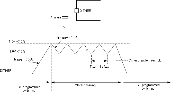
The device provides an optional programmable spread spectrum (clock dithering) function that is activated by connecting a capacitor between DITHER and AGND. A triangular waveform centered at 1.0 V is generated across the dither capacitor. This triangular waveform modulates the oscillator frequency by –6% to +5% of the frequency set by the RT resistor. The dither capacitance value sets the rate of the low frequency modulation.
 Figure 9-10 Switching Frequency
Dithering
Figure 9-10 Switching Frequency
DitheringFor the dithering circuit to effectively reduce peak EMI, the modulation frequency must be much less than the RT switching frequency. The dither capacitance, which is required for a given modulation frequency (fMOD), can be calculated from Equation 8. Setting the fMOD to 9 kHz or 10 kHz is a good starting point.
Connecting DITHER to AGND deactivates clock dithering, and the internal oscillator operates at a fixed frequency set by the RT resistor. Clock dithering is also disabled when an external synchronization pulse is applied.
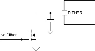
 Figure 9-11 Dynamic Dither On/Off
Example
Figure 9-11 Dynamic Dither On/Off
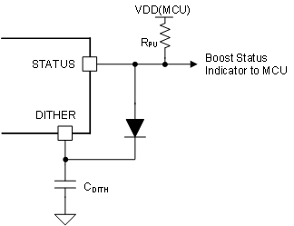
ExampleConnecting STATUS to DITHER enables the clock dithering when the STATUS pin is pulled down to ground and also enables the internal charge pump during bypass operation when the STATUS pin is pulled up.
 Figure 9-12 Enable Clock Dithering and Internal Charge Pump Together