ZHCSPX4A February 2022 – April 2022 LM5152-Q1 , LM51521-Q1
PRODUCTION DATA
- 1 特性
- 2 应用
- 3 说明
- 4 Revision History
- 5 说明(续)
- 6 Device Comparison Table
- 7 Pin Configuration and Functions
- 8 Specifications
-
9 Detailed Description
- 9.1 Overview
- 9.2 Functional Block Diagram
- 9.3
Feature Description
- 9.3.1 Device Enable/Disable (EN, VH Pin)
- 9.3.2 High Voltage VCC Regulator (BIAS, VCC Pin)
- 9.3.3 Light Load Switching Mode Selection (MODE Pin)
- 9.3.4 Line Undervoltage Lockout (UVLO Pin)
- 9.3.5 Fast Restart Using VCC HOLD (VH Pin)
- 9.3.6 Adjustable Output Regulation Target (VOUT, TRK, VREF Pin)
- 9.3.7 Overvoltage Protection (VOUT Pin)
- 9.3.8 Boost Status Indicator (STATUS Pin)
- 9.3.9 Dynamically Programmable Switching Frequency (RT)
- 9.3.10 External Clock Synchronization (SYNC Pin)
- 9.3.11 Programmable Spread Spectrum (DITHER Pin)
- 9.3.12 Programmable Soft Start (SS Pin)
- 9.3.13 Wide Bandwidth Transconductance Error Amplifier and PWM (TRK, COMP Pin)
- 9.3.14 Current Sensing and Slope Compensation (CSP, CSN Pin)
- 9.3.15 Constant Peak Current Limit (CSP, CSN Pin)
- 9.3.16 Maximum Duty Cycle and Minimum Controllable On-Time Limits
- 9.3.17 Deep Sleep Mode and Bypass Operation (HO, CP Pin)
- 9.3.18 MOSFET Drivers, Integrated Boot Diode, and Hiccup Mode Fault Protection (LO, HO, HB Pin)
- 9.3.19 Thermal Shutdown Protection
- 9.4 Device Functional Modes
- 10Application and Implementation
- 11Power Supply Recommendations
- 12Layout
- 13Device and Documentation Support
- 14Mechanical, Packaging, and Orderable Information
9.3.13 Wide Bandwidth Transconductance Error Amplifier and PWM (TRK, COMP Pin)
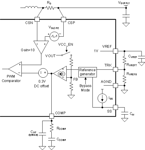
The device includes an internal feedback resistor voltage divider. The internal feedback resistor voltage divider is connected to the negative input of the internal transconductance error amplifier, and the TRK pin voltage programs the positive input of the internal transconductance error amplifier after the soft start is finished. The internal transconductance error amplifier features high output resistance (RO = 10 MΩ) and wide bandwidth (BW = 3 MHz) and sinks (or sources) current, which is proportional to the difference between the negative and the positive inputs of the error amplifier.
The output of the error amplifier is connected to the COMP pin, allowing the use of a Type-2 loop compensation network. RCOMP, CCOMP, and an optional CHF loop compensation components configure the error amplifier gain and phase characteristics to achieve a stable loop response. This compensation network creates a pole at very low frequency, a mid-band zero, and a high frequency pole.
The PWM comparator in Figure 9-14 compares the sum of the amplified sensed inductor current and the slope compensation ramp with the sum of the COMP pin voltage and a –0.3-V internal offset, and terminates the present cycle if the sum of the amplified sensed inductor current and the slope compensation ramp is greater than the sum of the COMP pin voltage and the –0.3-V internal offset.
 Figure 9-14 Error Amplifier, Current Sense
Amplifier, and PWM