ZHCSD65B SEPTEMBER 2013 – December 2014 LM5121 , LM5121-Q1
PRODUCTION DATA.
- 1 特性
- 2 应用
- 3 说明
- 4 修订历史记录
- 5 Pin Configuration and Functions
- 6 Specifications
-
7 Detailed Description
- 7.1 Overview
- 7.2 Functional Block Diagram
- 7.3
Feature Description
- 7.3.1 Undervoltage Lockout (UVLO)
- 7.3.2 High Voltage VCC Regulator
- 7.3.3 Oscillator
- 7.3.4 Slope Compensation
- 7.3.5 Error Amplifier
- 7.3.6 PWM Comparator
- 7.3.7 Disconnection Switch Control
- 7.3.8 Soft-Start
- 7.3.9 HO and LO Drivers
- 7.3.10 Bypass Operation (VOUT = VIN)
- 7.3.11 Cycle-by-Cycle Current Limit
- 7.3.12 Circuit Breaker Function
- 7.3.13 Clock Synchronization
- 7.3.14 Maximum Duty Cycle
- 7.3.15 Thermal Protection
- 7.4 Device Functional Modes
-
8 Application and Implementation
- 8.1 Application Information
- 8.2
Typical Application
- 8.2.1 Design Requirements
- 8.2.2
Detailed Design Procedure
- 8.2.2.1 Timing Resistor RT
- 8.2.2.2 UVLO Divider RUV2, RUV1
- 8.2.2.3 Input Inductor LIN
- 8.2.2.4 Current Sense Resistor RS
- 8.2.2.5 Current Sense Filter RCSFP, RCSFN, CCS
- 8.2.2.6 Slope Compensation Resistor RSLOPE
- 8.2.2.7 Output Capacitor COUT
- 8.2.2.8 Input Capacitor CIN
- 8.2.2.9 VIN Filter RVIN, CVIN
- 8.2.2.10 Bootstrap Capacitor CBST and Boost Diode DBST
- 8.2.2.11 VCC Capacitor CVCC
- 8.2.2.12 Output Voltage Divider RFB1, RFB2
- 8.2.2.13 Soft-Start Capacitor CSS
- 8.2.2.14 Restart Capacitor CRES
- 8.2.2.15 Low-Side Power Switch QL
- 8.2.2.16 High-Side Power Switch QH and Additional Parallel Schottky Diode
- 8.2.2.17 Snubber Components
- 8.2.2.18 Disconnect Switch QD Selection
- 8.2.2.19 Freewheeling Diode DF Selection
- 8.2.2.20 Loop Compensation Components CCOMP, RCOMP, CHF
- 8.2.3 Application Curves
- 9 Power Supply Recommendations
- 10Layout
- 11器件和文档支持
- 12机械封装和可订购信息
6 Specifications
6.1 Absolute Maximum Ratings(1)
Over operating free-air temperature range (unless otherwise noted)| MIN | MAX | UNIT | ||
|---|---|---|---|---|
| Input | VIN, CSP, CSN | –0.3 | 75 | V |
| BST to SW, FB, MODE, UVLO, VCC(2) | –0.3 | 15 | ||
| SW | –5.0 | 105 | ||
| BST | –0.3 | 115 | ||
| SS, SLOPE, SYNCIN/RT | –0.3 | 7 | ||
| CSP to CSN, PGND | –0.3 | 0.3 | ||
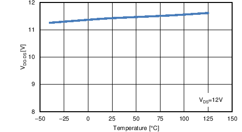
| Output(3) | DG to DS | –3.0 | 18 | |
| DG to VIN | –75 | 15 | ||
| DS | –3.0 | 75 | ||
| HO to SW | –0.3 | BST to SW+0.3 | ||
| LO | –0.3 | VCC+0.3 | ||
| COMP, RES | –0.3 | 7 | ||
| Thermal | Junction Temperature | –40 | 150 | ºC |
(1) Stresses beyond those listed under Absolute Maximum Ratings may cause permanent damage to the device. These are stress ratings only and functional operation of the device at these or any other conditions beyond those indicated under Recommended Operating Conditions are not implied. Exposure to absolute-maximum-rated conditions for extended periods may affect device reliability. Unless otherwise specified, all voltages are referenced to AGND pin.
(2) See Application Information when input supply voltage is less than the VCC voltage.
(3) All output pins are not specified to have an external voltage applied.
6.2 Handling Ratings: LM5121
| MIN | MAX | UNIT | |||
|---|---|---|---|---|---|
| Tstg | Storage temperature range | –55 | 150 | °C | |
| V(ESD) | Electrostatic discharge | Human body model (HBM), per JESD22-A114 | 2 | kV | |
| Charged device model (CDM), per JESD22-C101 | 1 | ||||
6.3 Handling Ratings: LM5121-Q1
| MIN | MAX | UNIT | ||||
|---|---|---|---|---|---|---|
| Tstg | Storage temperature range | –55 | 150 | °C | ||
| V(ESD) | Electrostatic discharge | Human body model (HBM), per AEC Q100-002(1) | –2 | 2 | kV | |
| Charged device model (CDM), per AEC Q100-011 | Corner pins (1, 10, 11, and 20) | –1 | 1 | |||
| Other pins | –1 | 1 | ||||
(1) AEC Q100-002 indicates HBM stressing is done in accordance with the ANSI/ESDA/JEDEC JS-001 specification.
6.4 Recommended Operating Conditions(1)
Over operating free-air temperature range (unless otherwise noted)| MIN | NOM | MAX | UNIT | ||
|---|---|---|---|---|---|
| Input supply voltage(2) | VIN | 4.5 | 65 | V | |
| Disconnection switch voltage(2) | DG, DS | 3.0 | 65 | ||
| Low-side driver bias voltage | VCC | 14 | |||
| High-side driver bias voltage | BST to SW | 3.8 | 14 | ||
| Current sense common mode range(2) | CSP, CSN | 3.0 | 65 | ||
| Switch node voltage | SW | 100 | |||
| Junction temperature | TJ | –40 | 125 | ºC | |
(1) Recommended Operating Conditions are conditions under which operation of the device is intended to be functional, but does not guarantee specific performance limits.
(2) Minimum VIN operating voltage is always 4.5 V. The minimum input power supply voltage can be 3.0 V after start-up, assuming VIN voltage is supplied from an available external source.
6.5 Thermal Information
| THERMAL METRIC(1) | LM5121, LM5121-Q1 |
UNIT | ||
|---|---|---|---|---|
| PWP | ||||
| 20 PINS | ||||
| RθJA | Junction-to-ambient thermal resistance (Typ.) | 40 | ºC/W | |
| RθJC(bot) | Junction-to-case (bot) thermal resistance (Typ.) | 4 | ºC/W | |
(1) For more information about traditional and new thermal metrics, see the IC Package Thermal Metrics application report, SPRA953.
6.6 Electrical Characteristics
Unless otherwise specified, these specifications apply for –40°C ≤ TJ ≤ +125°C, VVIN = 12 V, VVCC = 8.3 V, RT = 20 kΩ, no load on LO and HO. Typical values represent the most likely parametric norm at TJ = 25°C, and are provided for reference purposes only.| PARAMETER | TEST CONDITIONS | MIN | TYP | MAX | UNIT | ||
|---|---|---|---|---|---|---|---|
| VIN SUPPLY | |||||||
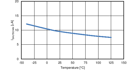
| ISHUTDOWN | VIN shutdown current | VUVLO = 0 V | 9 | 17 | µA | ||
| IBIAS | VIN operating current (exclude the current into RT resistor) | VUVLO = 2 V, non-switching | 4 | 5 | mA | ||
| VCC REGULATOR | |||||||
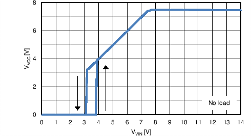
| VCC(REG) | VCC regulation | No load | 6.9 | 7.6 | 8.3 | V | |
| VCC dropout (VIN to VCC) | VVIN = 4.5 V, no external load | 0.25 | |||||
| VVIN = 4.5 V, IVCC = 25 mA | 0.28 | 0.5 | |||||
| VCC sourcing current limit | VVCC = 0 V | 50 | 62 | mA | |||
| IVCC | VCC operating current (exclude the current into RT resistor) | VVCC = 8.3 V | 3.5 | 5 | |||
| VVCC = 12 V | 4.5 | 8 | |||||
| VCC undervoltage threshold | VCC rising, VVIN = 4.5 V | 3.9 | 4.0 | 4.1 | V | ||
| VCC falling, VVIN = 4.5 V | 3.7 | ||||||
| VCC undervoltage hysteresis | 0.385 | ||||||
| UNDERVOLTAGE LOCKOUT | |||||||
| UVLO threshold | UVLO rising | 1.17 | 1.20 | 1.23 | V | ||
| UVLO hysteresis current | VUVLO = 1.4 V | 7 | 10 | 13 | µA | ||
| UVLO standby threshold | UVLO rising | 0.3 | 0.4 | 0.5 | V | ||
| UVLO standby hysteresis | 0.1 | 0.125 | |||||
| MODE | |||||||
| Diode emulation mode threshold | MODE rising | 1.20 | 1.24 | 1.28 | V | ||
| Diode emulation mode hysteresis | 0.1 | ||||||
| Default MODE voltage | 145 | 155 | 170 | mV | |||
| Default skip cycle threshold | COMP rising, measured at COMP | 1.290 | V | ||||
| COMP falling, measured at COMP | 1.245 | ||||||
| Skip cycle hysteresis | Measured at COMP | 40 | mV | ||||
| ERROR AMPLIFIER | |||||||
| VREF | FB reference voltage | Measured at FB, VFB= VCOMP | 1.188 | 1.200 | 1.212 | V | |
| FB input bias current | VFB= VREF | 5 | nA | ||||
| VOH | COMP output high voltage | ISOURCE = 2 mA, VVCC = 4.5 V | 2.75 | V | |||
| ISOURCE = 2 mA, VVCC = 12 V | 3.40 | ||||||
| VOL | COMP output low voltage | ISINK = 2 mA | 0.25 | ||||
| AOL | DC gain | 80 | dB | ||||
| fBW | Unity gain bandwidth | 3 | MHz | ||||
| OSCILLATOR | |||||||
| fSW1 | Switching frequency 1 | RT = 20 kΩ | 400 | 450 | 500 | kHz | |
| fSW2 | Switching frequency 2 | RT = 10 kΩ | 775 | 875 | 975 | ||
| RT output voltage | 1.2 | V | |||||
| RT sync rising threshold | RT rising | 2.5 | 2.9 | ||||
| RT sync falling threshold | RT falling | 1.6 | 2.0 | ||||
| Minimum sync pulse width | 100 | ns | |||||
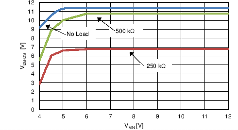
| DISCONNECTION SWITCH CONTROL | |||||||
| IDIS-SOURCE | DG current source | UVLO = 2 V, Sourcing | 25 | uA | |||
| IDIS-SINK | DG current sink | Inrush Control, Sinking | 67 | ||||
| DG discharge switch RDS-ON | Circuit Breaker | 38 | Ω | ||||
| DG charge pump regulation | DG to VIN, No load, VVIN = 4.5 V | 9.5 | 10.5 | 11.5 | V | ||
| DG to VIN, No load, VVIN = 12 V | 12.5 | ||||||
| VGS-DET | VGS detection threshold | DG to DS, Rising, VVIN = 12 V | 4.0 | 5.4 | 6.5 | ||
| VGS detection hysteresis | 0.2 | ||||||
| Transconductance gain | CSP to CSN to IDG | 12 | uA/mV | ||||
| SLOPE COMPENSATION | |||||||
| SLOPE output voltage | 1.17 | 1.20 | 1.23 | V | |||
| VSLOPE | Slope compensation amplitude | RSLOPE = 20 kΩ, fSW = 100 kHz, 50% duty cycle, TJ = –40ºC to +125ºC | 1.375 | 1.650 | 1.925 | ||
| RSLOPE= 20 kΩ, fSW= 100 kHz, 50% duty cycle, TJ = 25ºC | 1.400 | 1.650 | 1.900 | ||||
| SOFT-START | |||||||
| ISS-SOURCE | SS current source | VSS = 0 V | 7.5 | 10 | 12 | µA | |
| SS discharge switch RDS-ON | 13 | Ω | |||||
| PWM COMPARATOR | |||||||
| tLO-OFF | Forced LO off-time | VVCC = 5.5 V | 420 | 550 | ns | ||
| VVCC = 4.5 V | 360 | 500 | |||||
| tON-MIN | Minimum LO on-time | RSLOPE = 20 kΩ | 150 | ||||
| RSLOPE = 200 kΩ | 300 | ||||||
| COMP to PWM voltage drop | TJ = –40ºC to +125ºC | 0.95 | 1.10 | 1.25 | V | ||
| TJ = 25ºC | 1.00 | 1.10 | 1.20 | ||||
| CURRENT SENSE / CYCLE-BY-CYCLE CURRENT LIMIT | |||||||
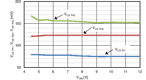
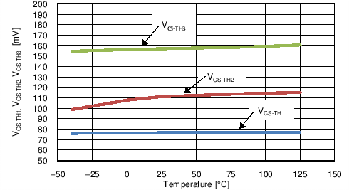
| VCS-TH1 | Cycle-by-cycle current limit threshold | CSP to CSN, TJ = –40ºC to +125ºC | 65.5 | 75.0 | 87.5 | mV | |
| CSP to CSN, TJ = 25ºC | 67.0 | 75.0 | 86.0 | ||||
| VCS-TH2 –VCS-TH1 | 5 | ||||||
| VCS-TH2 | Inrush current limit threshold | CSP to CSN | 80 | 110 | 133 | ||
| VCS-TH3 | Circuit breaker enable threshold | CSP to CSN, Rising | 143 | 160 | 170 | ||
| VCS-TH3 – VCS-TH2 | 20 | ||||||
| VCS-TH4 | Circuit breaker disable threshold | CSP to CSN, Falling | 4.0 | 11.5 | 16.0 | ||
| VCS-ZCD | Zero cross detection threshold | CSP to CSN, Rising | 7 | ||||
| CSP to CSN, Falling | 0.3 | 6 | 12 | ||||
| Current sense amplifier gain | 10 | V/V | |||||
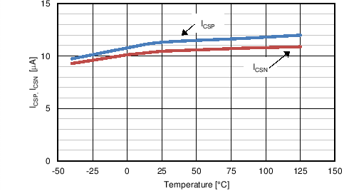
| ICSP | CSP input bias current | 12 | µA | ||||
| ICSN | CSN input bias current | 11 | |||||
| Bias current matching | ICSP to ICSN | –1.75 | 1 | 3.75 | |||
| CS to LO delay | Current sense / current limit delay | 150 | ns | ||||
| HICCUP MODE RESTART | |||||||
| VRES | Restart threshold | RES rising | 1.15 | 1.20 | 1.25 | V | |
| VHCP-UPPER | Hiccup counter upper threshold | RES rising | 4.2 | ||||
| RES rising, VVIN = VVCC = 4.5 V | 3.6 | ||||||
| VHCP-LOWER | Hiccup counter lower threshold | RES falling | 2.15 | ||||
| RES falling, VVIN = VVCC = 4.5 V | 1.85 | ||||||
| IRES-SOURCE1 | RES current source1 | Fault-state charging current | 20 | 30 | 40 | µA | |
| IRES-SINK1 | RES current sink1 | Normal-state discharging current | 5 | ||||
| IRES-SOURCE2 | RES current source2 | Hiccup mode off-time charging current | 10 | ||||
| IRES-SINK2 | RES current sink2 | Hiccup mode off-time discharging current | 5 | ||||
| Hiccup cycle | 8 | Cycles | |||||
| RES discharge switch RDS-ON | 40 | Ω | |||||
| Ratio of hiccup mode off-time to restart delay time | 122 | ||||||
| HO GATE DRIVER | |||||||
| VOHH | HO high-state voltage drop | IHO = –100 mA, VOHH = VBST – VHO | 0.15 | 0.24 | V | ||
| VOLH | HO low-state voltage drop | IHO = 100 mA, VOLH = VHO – VSW | 0.1 | 0.18 | |||
| HO rise time (10% to 90%) | CLOAD = 4700 pF, VBST = 12 V | 25 | ns | ||||
| HO fall time (90% to 10%) | CLOAD = 4700 pF, VBST = 12 V | 20 | |||||
| IOHH | Peak HO source current | VHO = 0 V, VSW = 0 V, VBST = 4.5 V | 0.8 | A | |||
| VHO = 0 V, VSW = 0 V, VBST = 7.6 V | 1.9 | ||||||
| IOLH | Peak HO sink current | VHO = VBST = 4.5 V | 1.9 | ||||
| VHO = VBST = 7.6 V | 3.2 | ||||||
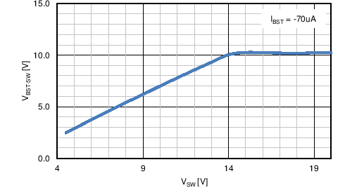
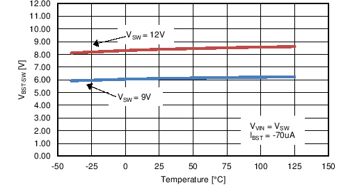
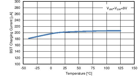
| IBST | BST charge pump sourcing current | VVIN = VSW = 9.0 V , VBST - VSW = 5.0 V | 90 | 200 | µA | ||
| BST charge pump regulation | BST to SW, IBST= –70 μA, VVIN = VSW = 9.0 V |
5.3 | 6.2 | 6.75 | V | ||
| BST to SW, IBST = –70 μA, VVIN = VSW = 12 V |
7 | 8.5 | 9 | ||||
| BST to SW undervoltage | 2.0 | 3.0 | 3.5 | ||||
| BST DC bias current | VBST - VSW = 12 V, VSW = 0 V | 30 | 45 | µA | |||
| LO GATE DRIVER | |||||||
| VOHL | LO high-state voltage drop | ILO = –100 mA, VOHL = VVCC – VLO | 0.15 | 0.25 | V | ||
| VOLL | LO low-state voltage drop | ILO = 100 mA, VOLL = VLO | 0.1 | 0.17 | |||
| LO rise time (10% to 90%) | CLOAD = 4700 pF | 25 | ns | ||||
| LO fall time (90% to 10%) | CLOAD = 4700 pF | 20 | |||||
| IOHL | Peak LO source current | VLO = 0 V, VVCC = 4.5 V | 0.8 | A | |||
| VLO = 0 V | 2.0 | ||||||
| IOLL | Peak LO sink current | VLO = VVCC = 4.5 V | 1.8 | ||||
| VLO = VVCC | 3.2 | ||||||
| SWITCHING CHARACTERISTICS | |||||||
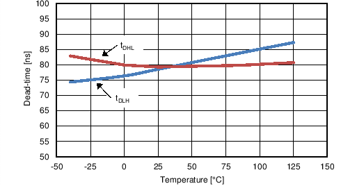
| tDLH | LO fall to HO rise delay | No load, 50% to 50% | 50 | 80 | 115 | ns | |
| tDHL | HO fall to LO rise delay | No load, 50% to 50% | 60 | 80 | 105 | ||
| THERMAL | |||||||
| TSD | Thermal shutdown | Temperature rising | 165 | ºC | |||
| Thermal shutdown hysteresis | 25 | ||||||
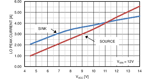
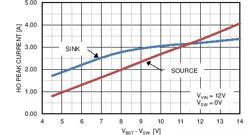
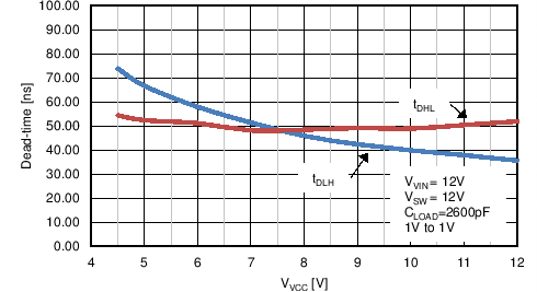
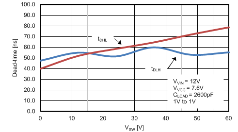
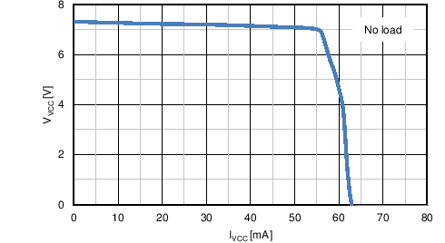
6.7 Typical Characteristics
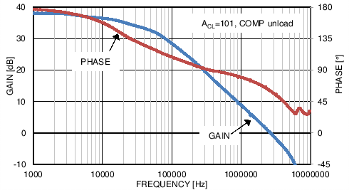
and Phase vs Frequency