ZHCSD65B SEPTEMBER 2013 – December 2014 LM5121 , LM5121-Q1
PRODUCTION DATA.
- 1 特性
- 2 应用
- 3 说明
- 4 修订历史记录
- 5 Pin Configuration and Functions
- 6 Specifications
-
7 Detailed Description
- 7.1 Overview
- 7.2 Functional Block Diagram
- 7.3
Feature Description
- 7.3.1 Undervoltage Lockout (UVLO)
- 7.3.2 High Voltage VCC Regulator
- 7.3.3 Oscillator
- 7.3.4 Slope Compensation
- 7.3.5 Error Amplifier
- 7.3.6 PWM Comparator
- 7.3.7 Disconnection Switch Control
- 7.3.8 Soft-Start
- 7.3.9 HO and LO Drivers
- 7.3.10 Bypass Operation (VOUT = VIN)
- 7.3.11 Cycle-by-Cycle Current Limit
- 7.3.12 Circuit Breaker Function
- 7.3.13 Clock Synchronization
- 7.3.14 Maximum Duty Cycle
- 7.3.15 Thermal Protection
- 7.4 Device Functional Modes
-
8 Application and Implementation
- 8.1 Application Information
- 8.2
Typical Application
- 8.2.1 Design Requirements
- 8.2.2
Detailed Design Procedure
- 8.2.2.1 Timing Resistor RT
- 8.2.2.2 UVLO Divider RUV2, RUV1
- 8.2.2.3 Input Inductor LIN
- 8.2.2.4 Current Sense Resistor RS
- 8.2.2.5 Current Sense Filter RCSFP, RCSFN, CCS
- 8.2.2.6 Slope Compensation Resistor RSLOPE
- 8.2.2.7 Output Capacitor COUT
- 8.2.2.8 Input Capacitor CIN
- 8.2.2.9 VIN Filter RVIN, CVIN
- 8.2.2.10 Bootstrap Capacitor CBST and Boost Diode DBST
- 8.2.2.11 VCC Capacitor CVCC
- 8.2.2.12 Output Voltage Divider RFB1, RFB2
- 8.2.2.13 Soft-Start Capacitor CSS
- 8.2.2.14 Restart Capacitor CRES
- 8.2.2.15 Low-Side Power Switch QL
- 8.2.2.16 High-Side Power Switch QH and Additional Parallel Schottky Diode
- 8.2.2.17 Snubber Components
- 8.2.2.18 Disconnect Switch QD Selection
- 8.2.2.19 Freewheeling Diode DF Selection
- 8.2.2.20 Loop Compensation Components CCOMP, RCOMP, CHF
- 8.2.3 Application Curves
- 9 Power Supply Recommendations
- 10Layout
- 11器件和文档支持
- 12机械封装和可订购信息
10 Layout
10.1 Layout Guidelines
In a boost regulator, the primary switching loop consists of the output capacitor and N-channel MOSFET power switches. Minimizing the area of this loop reduces the stray inductance and minimizes noise. Especially, placing high quality ceramic output capacitors as close to this loop earlier than bulk aluminum output capacitors minimizes output voltage ripple and ripple current of the aluminum capacitors.
In order to prevent a dv/dt induced turn-on of high-side switch, HO and SW should be connected to the gate and source of the high-side synchronous N-channel MOSFET switch through short and low inductance paths. In FPWM mode, the dv/dt induced turn-on can occur on the low-side switch. LO and PGND should be connected to the gate and source of the low-side N-channel MOSFET through short and low inductance paths. All of the power ground connections should be connected to a single point. Also, all of the noise sensitive low power ground connections should be connected together near the AGND pin and a single connection should be made to the single point PGND. CSP and CSN are high impedance pins and noise sensitive. CSP and CSN traces should be routed together with kelvin connections to the current sense resistor as short as possible. If needed, place 100-pF ceramic filter capacitor as close to the device. MODE pin is also high impedance and noise sensitive. If an external pull-up or pull-down resistor is used at MODE pin, the resistor should be placed as close the device. VCC, VIN and BST capacitor must be as physically close as possible to the device.
The LM5121 has an exposed thermal pad to aid power dissipation. Adding several vias under the exposed pad helps conduct heat away from the device. The junction to ambient thermal resistance varies with application. The most significant variables are the area of copper in the PC board, the number of vias under the exposed pad and the amount of forced air cooling. The integrity of the solder connection from the device exposed pad to the PC board is critical. Excessive voids greatly decrease the thermal dissipation capacity. The highest power dissipating components are the two power switches. Selecting N-channel MOSFET switches with exposed pads aids the power dissipation of these devices.
10.2 Layout Example
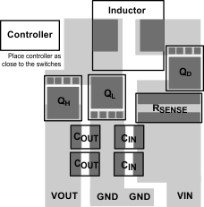 Figure 47. Power Path Layout