SNVS790F January 2012 – November 2015 LM5114
PRODUCTION DATA.
- 1 Features
- 2 Applications
- 3 Description
- 4 Revision History
- 5 Device Comparison Table
- 6 Pin Configuration and Functions
- 7 Specifications
- 8 Detailed Description
- 9 Application and Implementation
- 10Power Supply Recommendations
- 11Layout
- 12Device and Documentation Support
- 13Mechanical, Packaging, and Orderable Information
9 Application and Implementation
NOTE
Information in the following applications sections is not part of the TI component specification, and TI does not warrant its accuracy or completeness. TI’s customers are responsible for determining suitability of components for their purposes. Customers should validate and test their design implementation to confirm system functionality.
9.1 Application Information
The LM5114 has the features necessary to drive low-side enhancement mode GaN FETs. Due to the fast switching speed and relatively low gate voltage of enhancement mode GaN FETs, PCB layout is crucial to achieve reliable operation. Refer to Figure 32 for details.
9.2 Typical Application
Boost DC-DC converter using a 100-V enhancement mode GaN FET (EPC2001) as the boost power switch. The control circuitry is implemented with the LM5114, a 100-V current mode PWM controller.
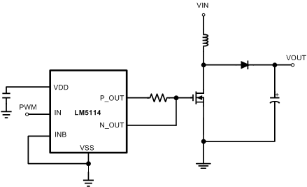 Figure 22. Simplified Boost Converter
9.2.1 Design Requirements
See Table 2 for the parameter and values.
Table 2. Operating Parameters
| PARAMETER | VALUE |
|---|---|
| Input Operating Voltage | 24 V to 66 V |
| Output Voltage | 75 V |
| Output Current | 2 A |
| Measured Efficiency | 97% @ at 48 V 2 A |
| Frequency of Operation | 500 kHz |
9.2.1.1 Power Dissipation
It is important to keep the power consumption of the driver below the maximum power dissipation limit of the package at the operating temperature. The total power dissipation of the LM5114 is the sum of the gate charge losses and the losses in the driver due to the internal CMOS stages used to buffer the output as well as the power losses associated with the quiescent current.
The gate charge losses can be calculated with the total input gate charge as in Equation 1 and Equation 2:

or

where
- Fsw is switching frequency
The power dissipation associated with the internal circuit operation of the driver can be estimated with the characterization curves of the LM5114. For a given ambient temperature, the maximum allowable power loss of the IC can be defined as Equation 3:

where
- P is the total power dissipation of the driver
This power PG is dissipated in the resistive elements of the circuit when the MOSFET/IGBT is being turned on and off. Half of the total power is dissipated when the load capacitor is charged during turnon, and the other half is dissipated when the load capacitor is discharged during turnoff. When no external gate resistor is employed between the driver and MOSFET/IGBT, this power is completely dissipated inside the driver package. With the use of external gate-drive resistors, the power dissipation is shared between the internal resistance of driver and external gate resistor.
9.2.1.1.1 Gate Drive
The enhancement mode GaN FETs have small gate capacitance and low threshold gate voltage. Therefore GaN FETs are prone to gate oscillations induced by PCB parasitic elements. It is necessary to place the driver as close to the GaN FET as possible to minimize the stray inductance. Gate resistors can be used to damp the oscillations and to adjust the switching speed. The LM5114 has split outputs, providing flexibility to adjust the turnon and turnoff strength independently. In the evaluation board, 1.5-Ω and 2.7-Ω gate resistors are used in the turnon and turnoff path respectively.
9.2.2 Detailed Design Procedure
The LM5114 has the features necessary to drive low-side enhancement mode GaN FETs. Due to the fast switching speed and relatively low gate voltage of enhancement mode GaN FETs, PCB layout is crucial to achieve reliable operation.
Generally, the switching speed of the power switch during turnon and turnoff should be as fast as possible in order to minimize switching power losses. The gate driver device must be able to provide the required peak current for achieving the targeted switching speeds with the targeted power switch. The system requirement for the switching speed is typically described in terms of the slew rate of the drain-to-source voltage of the power FET (such as dVDS/dt).
For example, the system requirement in this application might state that a EPC2001 GaN FET must be turned on with a dVDS/dt of 20 V/ns or higher with a DC bus voltage of 75 V.
This requirement means that the entire drain-to-source voltage swing during the FET turnon event (from 75 V in the OFF state to VDS(on) in on state) must be completed in approximately 3.75 ns or less. When the drain-to-source voltage swing occurs, the Miller charge of the power FET (QGD parameter in EPC2001 data sheet is
2.2 nC typical) is supplied by the peak current of gate driver. To achieve the targeted dVDS/dt, the gate driver must be capable of providing the QGD charge in 3.75 ns or less. In other words a peak current of 0.586 A
(= 2.2 nC / 2 ns) or higher must be provided by the gate driver.
The LM5114 gate driver is capable of providing 1.3-A peak sourcing current which clearly exceeds the design requirement and has the capability to meet the switching speed needed. The 2.2x overdrive capability provides an extra margin against part-to-part variations in the QGD parameter of the power MOSFET along with additional flexibility to insert external gate resistors and fine tune the switching speed for efficiency versus EMI optimizations. However, in practical designs the parasitic trace inductance in the gate drive circuit of the PCB will have a definitive role to play on the FET switching speed.
The effect of this trace inductance is to limit the dI/dt of the output current pulse of the gate driver. In order to illustrate this, consider output current pulse waveform from the gate driver to be approximated to a triangular profile, where the area under the triangle (½ × IPEAK × time) would equal the total gate charge of the power FET (QG parameter in the EPC2001 GaNFET datasheet = 8 nC typical). If the parasitic trace inductance limits the dI/dt then a situation may occur in which the full peak current capability of the gate driver is not fully achieved in the time required to deliver the QG required for the GaNFET switching. In other words the time parameter in the equation would dominate and the IPEAK value of the current pulse would be much less than the true peak current capability of the device, while the required QG is still delivered.
Because of this, the desired switching speed may not be realized, even when theoretical calculations indicate the gate driver is capable of achieving the targeted switching speed. Thus, placing the gate driver device very close to the power FET and designing a tight gate drive-loop with minimal PCB trace inductance is important to realize the full peak-current capability of the gate driver.
9.2.3 Application Curves
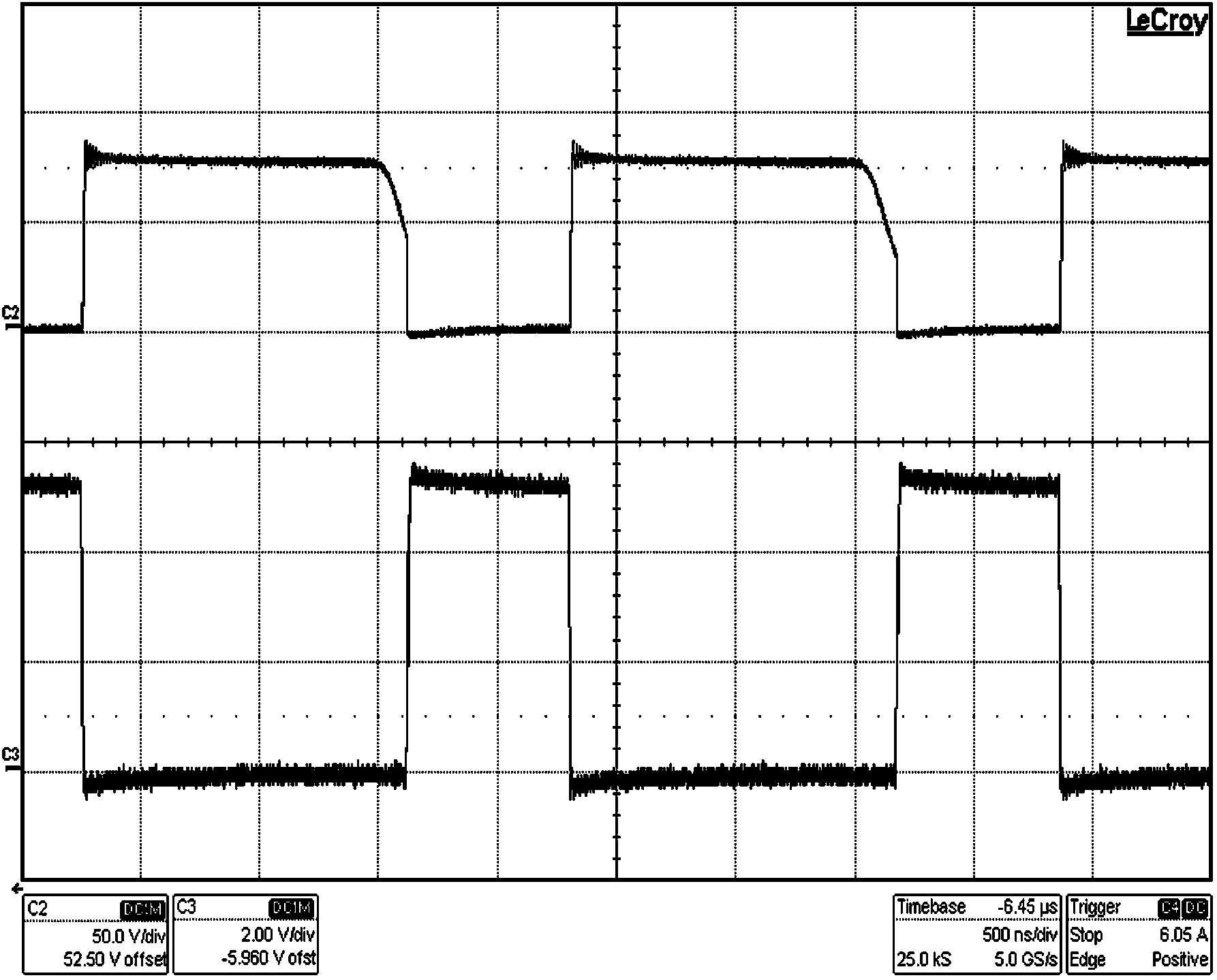
Input Voltage = 48 VDC, Load Current = 2 A
Traces:
Top Trace: Switch-node voltage, Volt/div = 50 V
Bottom Trace: Gate-Source Voltage of GaN FET, Volt/div = 2 V
Bandwidth Limit = 600 MHz
Horizontal Resolution = 500 ns/div
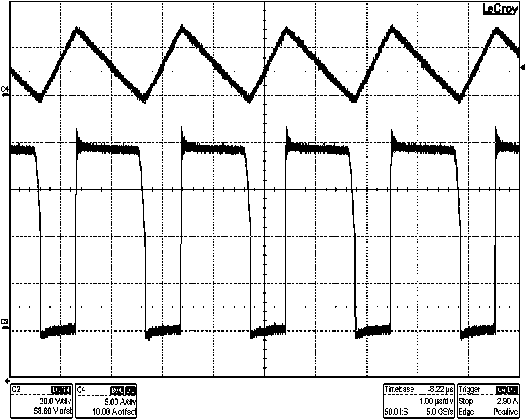
Input Voltage = 48 VDC
Load Current = 2 A
Traces:
Top Trace: Inductor Current, Amps/div = 5 A
Bottom Trace: Switch-Node Voltage, Volt/div = 20 V
Bandwidth Limit = 600 MHz
Horizontal Resolution = 1 µs/div
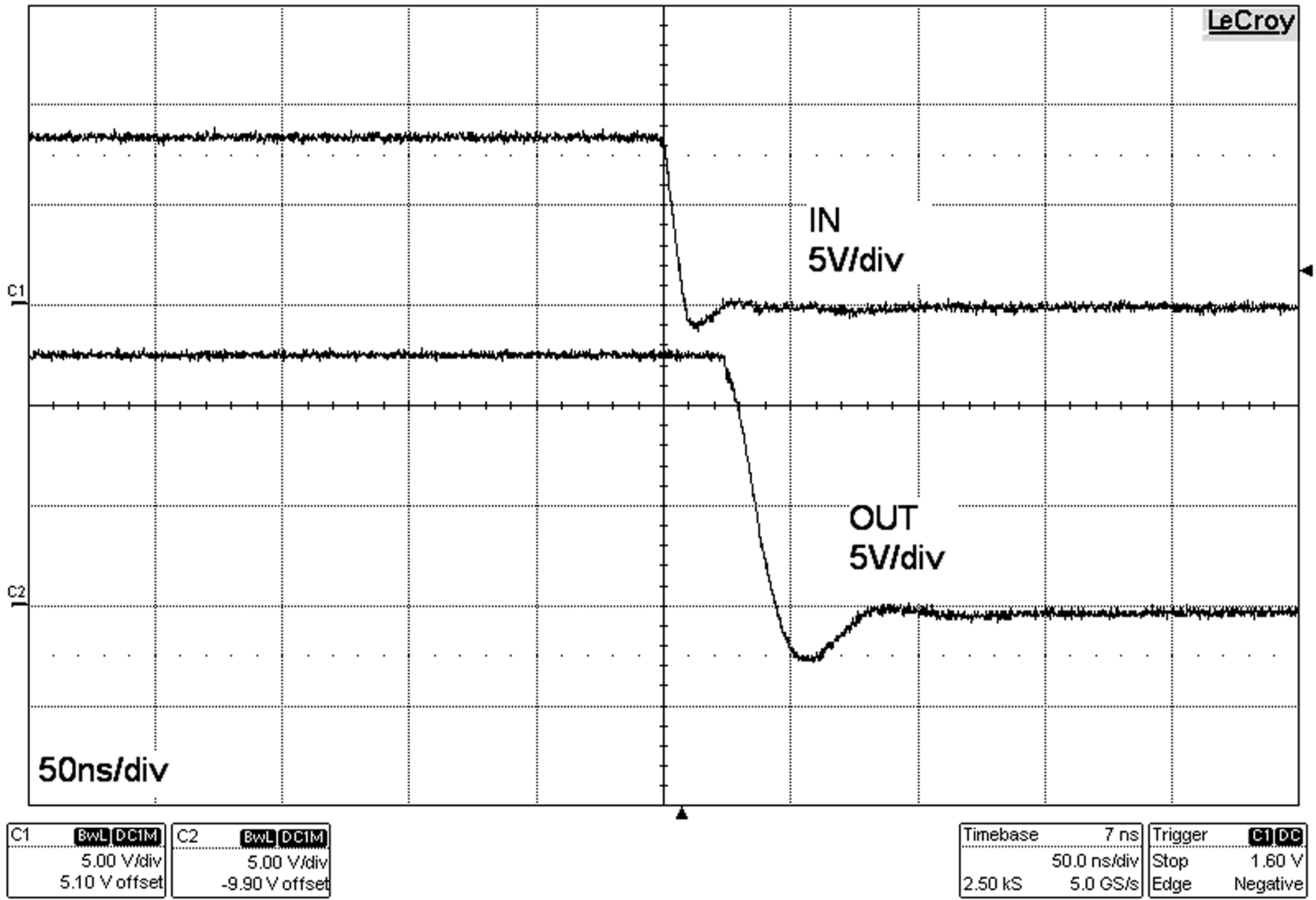 Figure 27. Input Voltage vs Output Voltage
(VDD = 12 V, CL = 10000 pF)
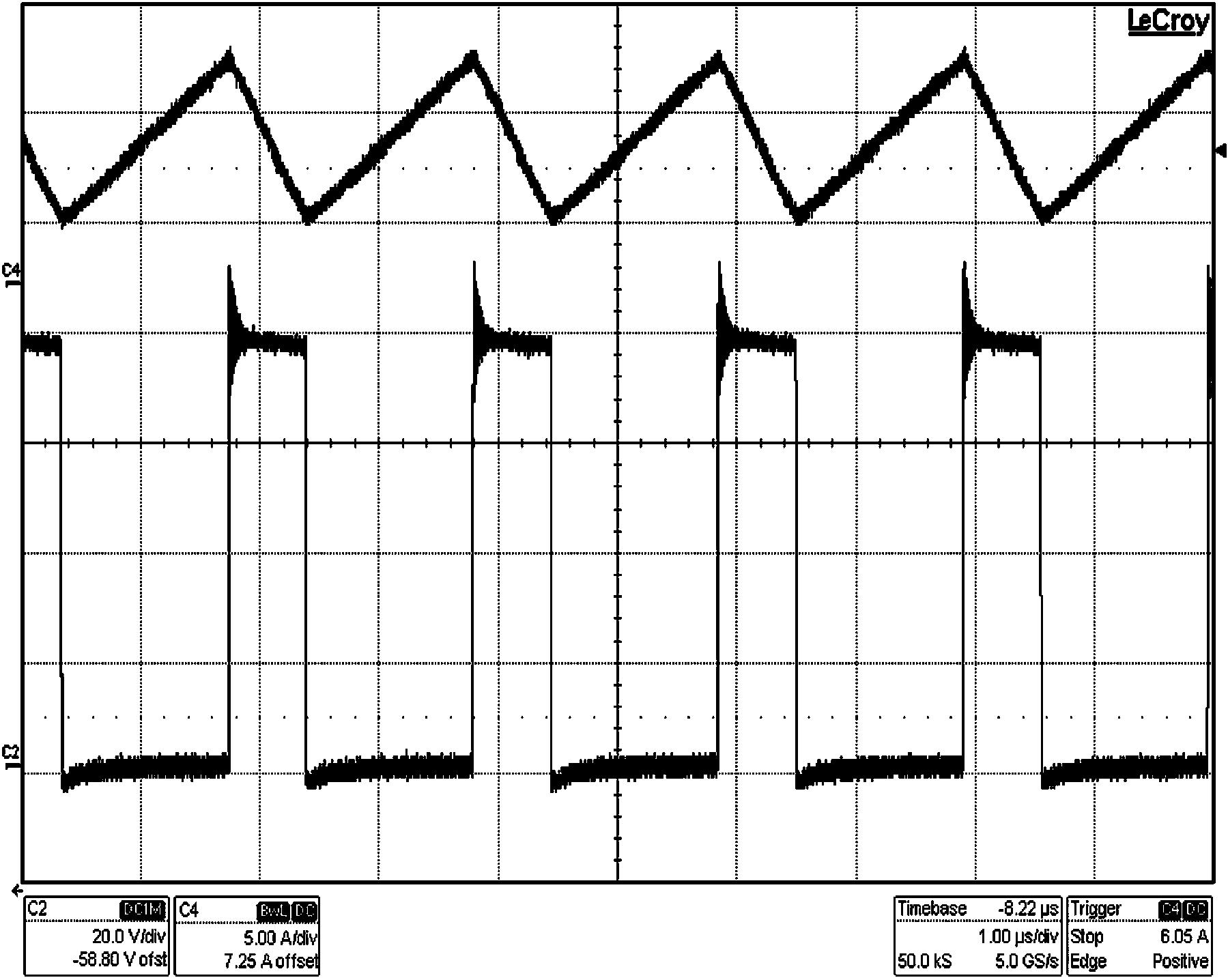
Input Voltage = 24 VDC, Load Current = 2 A
Traces:
Top Trace: Inductor Current, Amp/div = 5 A
Bottom Trace: Switch-Node Voltage, Volt/div = 20 V
Bandwidth Limit = 600 MHz
Horizontal Resolution = 1 µs/div
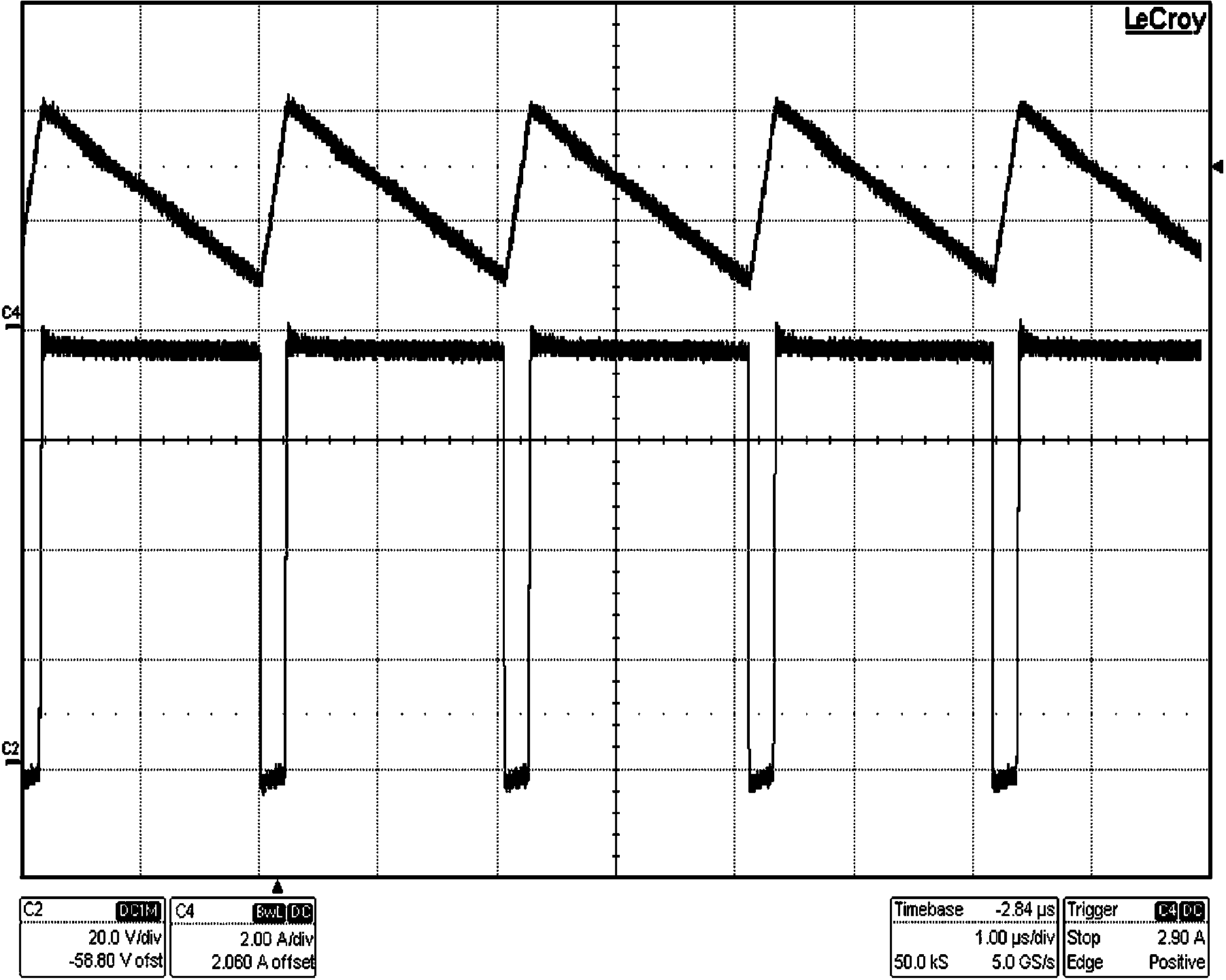
Input Voltage = 66 VDC
Load Current = 2 A
Traces:
Top Trace: Inductor Current, Amp/div = 5 A
Bottom Trace: Switch-Node Voltage, Volt/div = 20 V
Bandwidth Limit = 600 MHz
Horizontal Resolution = 1 µs/div
9.3 System Examples
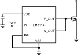 Figure 28. Noninverting Application
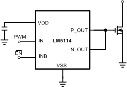 Figure 30. Noninverting Application
 With Enable Pin
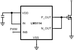 Figure 29. Inverting Application
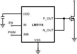 Figure 31. Inverting Application
 With Enable Pin