ZHCSEV7I June 2011 – October 2019 LM5113
PRODUCTION DATA.
- 1 特性
- 2 应用
- 3 说明
- 4 修订历史记录
- 5 Pin Configuration and Functions
- 6 Specifications
- 7 Detailed Description
- 8 Application and Implementation
- 9 Power Supply Recommendations
- 10Layout
- 11器件和文档支持
- 12机械、封装和可订购信息
封装选项
机械数据 (封装 | 引脚)
散热焊盘机械数据 (封装 | 引脚)
- DPR|10
订购信息
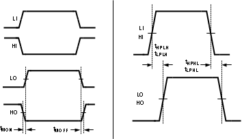
6.6 Switching Characteristics
over operating free-air temperature range (unless otherwise noted)| PARAMETER | TEST CONDITIONS | MIN | TYP | MAX | UNIT | ||
|---|---|---|---|---|---|---|---|
| tLPHL | LO turnoff propagation delay | LI falling to LOL falling | TJ = 25°C | 26.5 | ns | ||
| TJ = –40°C to 125°C | 45.0 | ||||||
| tLPLH | LO turnon propagation delay | LI rising to LOH rising | TJ = 25°C | 28.0 | ns | ||
| TJ = –40°C to 125°C | 45.0 | ||||||
| tHPHL | HO turnoff propagation delay | HI falling to HOL falling | TJ = 25°C | 26.5 | ns | ||
| TJ = –40°C to 125°C | 45.0 | ||||||
| tHPLH | HO turnon propagation delay | HI rising to HOH rising | TJ = 25°C | 28.0 | ns | ||
| TJ = –40°C to 125°C | 45.0 | ||||||
| tMON | Delay matching
LO on & HO off |
TJ = 25°C | 1.5 | ns | |||
| TJ = –40°C to 125°C | 8.0 | ||||||
| tMOFF | Delay matching
LO off & HO on |
TJ = 25°C | 1.5 | ns | |||
| TJ = –40°C to 125°C | 8.0 | ||||||
| tHRC | HO rise time (0.5 V – 4.5 V) | CL = 1000 pF | 7.0 | ns | |||
| tLRC | LO rise time (0.5 V – 4.5 V) | CL = 1000 pF | 7.0 | ns | |||
| tHFC | HO fall time (0.5 V – 4.5 V) | CL = 1000 pF | 1.5 | ns | |||
| tLFC | LO fall time (0.5 V – 4.5 V) | CL = 1000 pF | 1.5 | ns | |||
| tPW | Minimum input pulse width
that changes the output |
10 | ns | ||||
| tBS | Bootstrap diode
reverse recovery time |
IF = 100 mA, IR = 100 mA | 40 | ns | |||
(1) Minimum and maximum limits are 100% production tested at 25°C. Limits over the operating temperature range are ensured through correlation using Statistical Quality Control (SQC) methods. Limits are used to calculate Average Outgoing Quality Level (AOQL).
 Figure 1. Timing Diagram