ZHCSCJ2 June 2014 LM3633
PRODUCTION DATA.
- 1 特性
- 2 应用范围
- 3 说明
- 4 修订历史记录
- 5 Pin Configuration and Functions
- 6 Specifications
-
7 Detailed Description
- 7.1 Overview
- 7.2 Functional Block Diagram
- 7.3 Feature Description
- 7.4
Device Functional Modes
- 7.4.1
High-Voltage LED Control
- 7.4.1.1 High-Voltage Boost Converter
- 7.4.1.2 High-Voltage Current Sinks (HVLED1, HVLED2 and HVLED3)
- 7.4.1.3 High-Voltage Current String Biasing
- 7.4.1.4 Boost Switching-Frequency Select
- 7.4.1.5 Automatic Switching Frequency Shift
- 7.4.1.6 Brightness Register Current Control
- 7.4.1.7 PWM Control
- 7.4.1.8 Start-up/Shutdown Ramp
- 7.4.1.9 Run-Time Ramp
- 7.4.1.10 High-Voltage Control A/B Ramp Select
- 7.4.1.11 LED Current Mapping Modes
- 7.4.1.12 Exponential Mapping
- 7.4.1.13 Linear Mapping
- 7.4.2
Low-Voltage LED Control
- 7.4.2.1 Integrated Charge Pump
- 7.4.2.2 Charge Pump Disabled
- 7.4.2.3 Automatic Gain
- 7.4.2.4 Automatic Gain (Flying Capacitor Detection)
- 7.4.2.5 1X Gain
- 7.4.2.6 2X Gain
- 7.4.2.7 Low-Voltage Current Sinks (LVLED1 to LVLED6)
- 7.4.2.8 Low-Voltage LED Biasing
- 7.4.2.9 Brightness Register Current Control
- 7.4.2.10 LED Current Mapping Modes
- 7.4.2.11 Exponential Mapping
- 7.4.2.12 Linear Mapping
- 7.4.2.13 Start-up/Shutdown Ramp
- 7.4.2.14 Run-Time Ramp
- 7.4.3 Low-Voltage LED Pattern Generator
- 7.4.4 Fault Flags/Protection Features
- 7.4.5 I2C-Compatible Interface
- 7.4.1
High-Voltage LED Control
- 7.5 Register Descriptions
-
8 Applications and Implementation
- 8.1 Application Information
- 8.2
Typical Application
- 8.2.1 Design Requirements
- 8.2.2
Detailed Design Procedure
- 8.2.2.1 Boost Converter Maximum Output Power (Boost)
- 8.2.2.2 Boost Inductor Selection
- 8.2.2.3 Output Capacitor Selection
- 8.2.2.4 Schottky Diode Selection
- 8.2.2.5 Input Capacitor Selection
- 8.2.2.6 Maximum Output Power (Charge Pump)
- 8.2.2.7 Charge Pump Flying Capacitor Selection
- 8.2.2.8 Charge Pump Output Capacitor Selection
- 8.2.2.9 Charge Pump Input Capacitor Selection
- 8.2.3 Application Performance Plots
- 8.3 Initialization Set Up
- 9 Power Supply Recommendations
- 10Layout
- 11器件和文档支持
- 12机械封装和可订购信息
8 Applications and Implementation
8.1 Application Information
The LM3633 provides a complete high-performance, high-voltage LED and low-voltage-indicator LED lighting solution for mobile handsets. The LM3633 is highly configurable and can support the high-voltage LED configurations summarized in Table 36. The LM3633 utilizes internal ramp-time generators to provide smooth 11-bit high-voltage LED dimming while requiring only an 8-bit command from the host controller. The LM3633EVM is available with GUI software to aid understanding of the LM3633 operation.
Table 36. Supported High-Voltage LED Configurations
| NUMBER OF HIGH-VOLTAGE LED STRINGS | MAXIMUM NUMBER OF SERIES HIGH-VOLTAGE LEDs | |||
|---|---|---|---|---|
| 3 | 6 | |||
| 2 | 10 | |||
| 1 | 10 | |||
8.2 Typical Application
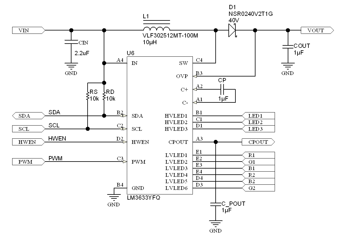 Figure 23. LM3633 Simplified Schematic
Table 37. Application Circuit Component List
| COMPONENT | MANUFACTURER | VALUE | PART NUMBER | SIZE | CURRENT/VOLTAGE RATING (Resistance) |
|---|---|---|---|---|---|
| L | TDK | 10 µH | VLF302512MT-100M | 2.5mm x 3.0mm x 1.2mm | 620 mA/0.25 mΩ |
| COUT | 1 µF | C2012X5R1H105 | 0805 | 50 V | |
| CIN | 2.2 µF | C1005X5R1A225 | 0402 | 10 V | |
| CPOUT/CP | 1 µF | C1005X5R1A105 | 0402 | 10 V | |
| WLED | 312WBCW(A) | 0603 | 30 mA/3.3 V (typ.) | ||
| Diode | On-Semi | NSR0240V2T1G | SOD-523 | 40 V, 250 mA |
8.2.1 Design Requirements
Table 38. Design Parameters
| DESIGN PARAMETER | EXAMPLE VALUE | |||
|---|---|---|---|---|
| Full-scale current setting | 20.2 mA | |||
| Minimum Input Voltage | 3.0 V | |||
| LED series/parallel configuration | 6s3p | |||
| LED maximum forward voltage (Vf) | 3.5 V | |||
| Efficiency | 80 | |||
The designer needs to know the following
- Full-scale current setting
- Minimum input voltage
- LED series/parallel configuration
- LED maximum Vf voltage
- LM3633 Efficiency for LED configuration
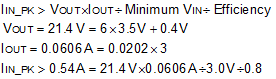
The full-scale current setting, number of led strings, number of series LEDs, and minimum input voltage are needed in order to calculate the peak input current. This information guides the designer to make the appropriate inductor selection for the application.
The LM3633 boost converter output voltage (VOUT) is calculated as follows: number of series LEDs * Vƒ + 0.4V
The LM3633 boost converter output current (IOUT) is calculated as follows: number of parallel LED strings * Full-scale current
The LM3633 peak input current (I IN_PK) is calculated as follows: VOUT * IOUT / Minimum VIN / Efficiency
8.2.2 Detailed Design Procedure
8.2.2.1 Boost Converter Maximum Output Power (Boost)
Maximum output power of the LM3633 is governed by two factors: the peak current limit (ICL = 880 mA min), and the maximum output voltage (VOVP). When the application causes either of these limits to be reached it is possible that the proper current regulation and matching between LED current strings is not met.
8.2.2.1.1 Peak Current Limited
In the case of a peak current limited situation, the NFET switch turns off for the remainder of the switching period when the inductor current peak hits the LM3633 current limit. If this happens each switching cycle the LM3633 regulates the inductor current peak instead of the headroom across the current sinks. This can result in the dropout of the boost output connected current sinks, and the LED current dropping below its programmed level.
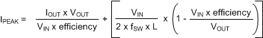
The peak current in a boost converter is dependent on the value of the inductor, total LED current in the boost (IOUT), the boost output voltage (VOUT) (which is the highest voltage LED string + VHR ), the input voltage (VIN), the switching frequency, and the efficiency (Output Power/Input Power). Additionally, the peak current is different depending on whether the inductor current is continuous during the entire switching period (CCM), or discontinuous (DCM) where it goes to 0 before the switching period ends. For Continuous Conduction Mode the peak inductor current is given by:
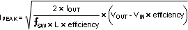
For Discontinuous Conduction Mode the peak inductor current is given by:
To determine which mode the circuit is operating in (CCM or DCM) it is necessary to perform a calculation to test whether the inductor current ripple is less than the anticipated input current (IIN). If ΔIL is less than IIN then the device operates in CCM. If ΔIL is greater than IIN then the device is operating in DCM.
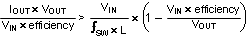
Typically at currents high enough to reach the LM3633 peak current limit, the device operates in CCM.
The following figures show the output current and voltage derating for a 10-µH and a 22-µH inductor. These plots take equations (1) and (2) from above and plot VOUT and IOUT with varying VIN, a constant peak current of 880 mA (ICL_MIN), 500-kHz switching frequency, and a constant efficiency of 85%. Using these curves gives a good design guideline on selecting the correct inductor for a given output power requirement. A 10-µH inductor is typically a smaller device with lower on resistance, but the peak currents are higher. A 22-µH inductor provides for lower peak currents, but to match the DC resistance of a 10-µH inductor, a larger-sized device is required.
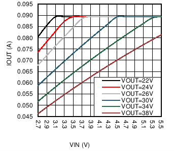 Figure 24. Maximum Output Power (22 µH)
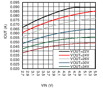 Figure 25. Maximum Output Power (10 µH)
8.2.2.1.2 Output Voltage Limited
In the case of a output voltage limited situation (VOUT = VOVP), when the boost output voltage hits the LM3633 OVP threshold, the NFET turns off and stays off until the output voltage falls below the hysteresis level (typically 1 V below the OVP threshold). This results in the boost converter regulating the output voltage to the programmed OVP threshold (16 V, 24 V, 32 V, or 40 V), causing the current sinks to go into dropout. The default OVP threshold is set at 16 V. For LED strings higher than typically 4 series LEDs, the OVP has to be programmed higher after power-up or after a HWEN reset.
8.2.2.2 Boost Inductor Selection
The boost circuit operates using a 4.7-μH to 22-μH inductor. The inductor selected must have a saturation current greater than the peak operating current.
8.2.2.3 Output Capacitor Selection
The LM3633 inductive boost converter requires a 1.0-µF (X5R or X7R) ceramic capacitor to filter the output voltage. The voltage rating of the capacitor depends on the selected OVP setting. For the 16-V setting a 16-V capacitor must be used. For the 24-V setting a 25-V capacitor must be used. For the 32-V setting, a 35-V capacitor must be used. For the 40-V setting a 50-V capacitor must be used. Pay careful attention to the capacitor tolerance and DC bias response. For proper operation the degradation in capacitance due to tolerance, DC bias, and temperature, should stay above 0.4 µF. This might require placing two devices in parallel in order to maintain the required output capacitance over the device operating range, and series LED configuration.
8.2.2.4 Schottky Diode Selection
The Schottky diode must have a reverse breakdown voltage greater than the LM3633 maximum output voltage (see Overvoltage Protection (Inductive Boost) section). Additionally, the diode must have an average current rating high enough to handle the LM3633 maximum output current, and at the same time the diode peak current rating must be high enough to handle the peak inductor current. Schottky diodes are required due to their lower forward voltage drop (0.3 V to 0.5 V) and their fast recovery time.
8.2.2.5 Input Capacitor Selection
The input capacitor on the LM3633 filters the voltage ripple due to the switching action of the inductive boost and the capacitive charge-pump doubler. A ceramic capacitor of at least 2.2-µF (X5R or X7R) must be used to filter the input voltage.
8.2.2.6 Maximum Output Power (Charge Pump)
The maximum output power available from the LM3633 charge pump is determined by the maximum output voltage available from the charge pump. In 1X gain the charge pump operates in Pass Mode so the voltage at CPOUT tracks VIN (less the drop across the charge-pump pass switch). In this case the maximum output power is given as:

where RCP is the resistance from VIN to CPOUT and ILVLED_TOTAL is the maximum programmed current in the LVLED strings.
In 2X gain the voltage at CPOUT (VCPOUT_2X) is regulated to typically 4.4 V. In this case the maximum output power is given by:

Both equations assume there is sufficient headroom at the top side of the low-voltage current sinks to ensure the LED current remains in regulation (VHR_LV) in the electrical table.
8.2.2.7 Charge Pump Flying Capacitor Selection
The charge pump flying capacitor must quickly charge up to the input voltage and then supply the current to the output every switching cycle (1 MHz). This fast switching action requires a 1.0-µF (X5R or X7R) ceramic capacitor connected to the C+ and C– pins with a low inductive connection.
8.2.2.8 Charge Pump Output Capacitor Selection
The charge pump output capacitor filters the switched charge from the flying capacitor every switching cycle (1 MHz). This fast switching action requires a 1.0-µF (X5R or X7R) ceramic capacitor connected to the CPOUT pin with a low-inductive connection.
8.2.2.9 Charge Pump Input Capacitor Selection
The input capacitor for the LM3633 charge pump is the same one used for the LM3633 inductive boost converter (see Input Capacitor Selection).
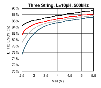
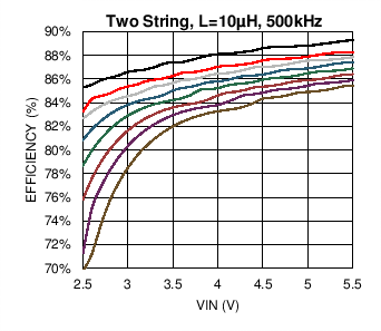
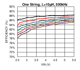
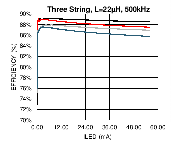
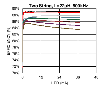
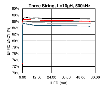
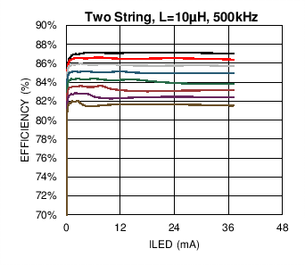
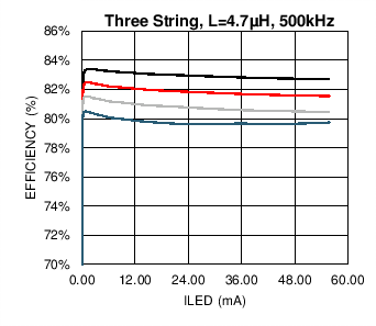
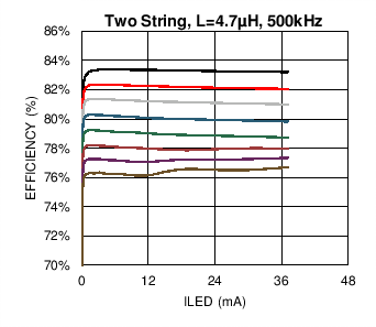
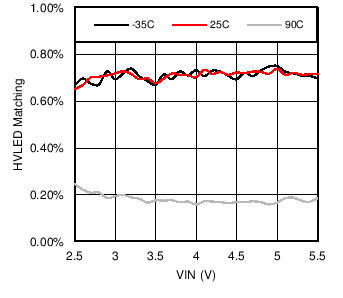
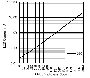
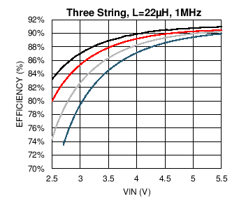
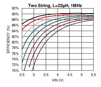
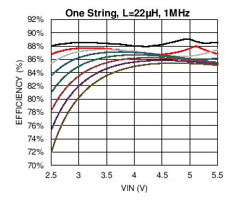
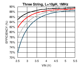
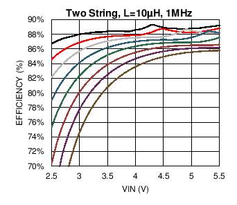
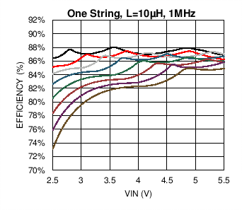
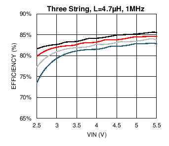
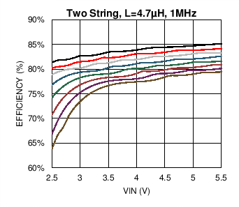
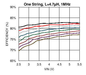
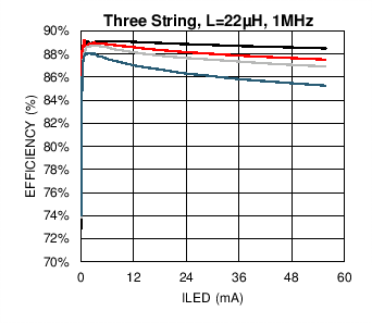
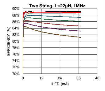
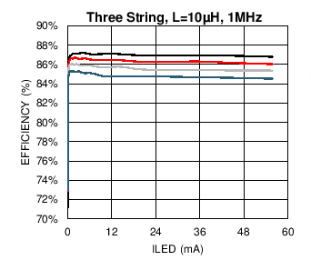
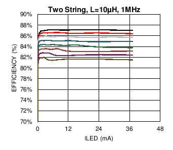
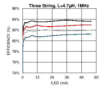
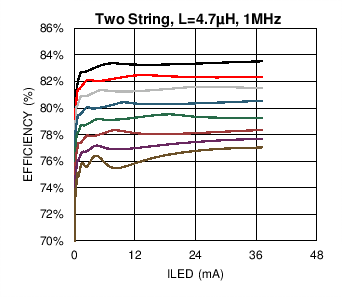
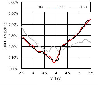
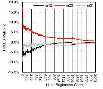
8.2.3 Application Performance Plots
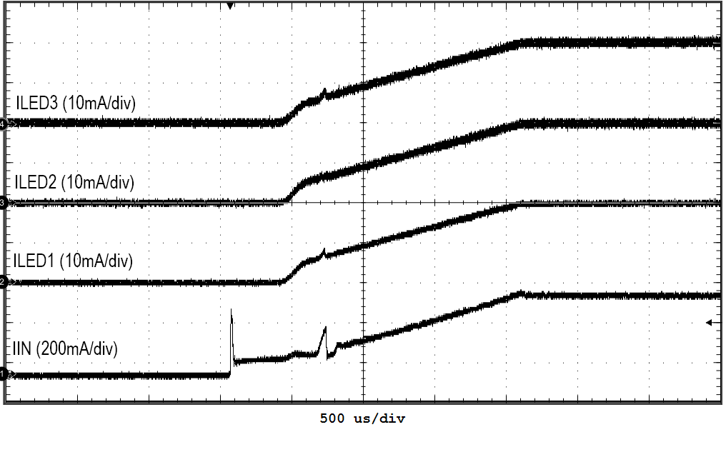
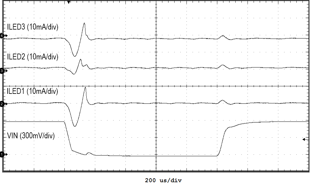
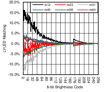
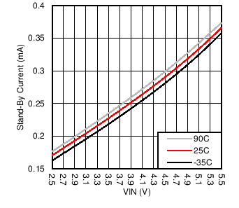
VIN = 3.6 V, VLED = 3.2 V @ 20 mA, Typical Application Circuit, TA = 25°C, Full-Scale Current = 20.2 mA unless otherwise specified. Efficiency is VOUT × (IHVLED1 + IHVLED2 + IHVLED3)/(VIN × IIN), matching curves are (ΔILED_MAX/ILED_AVE). See Table 37.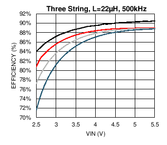
| Top to Bottom: 3x3, 3x4, 3x5, 3x6 (LEDs) |
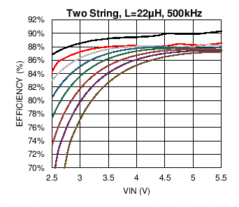
| Top to Bottom: 2x3, 2x4, 2x5, 2x6, 2x7, 2x8, 2x9, 2x10 (LEDs) |
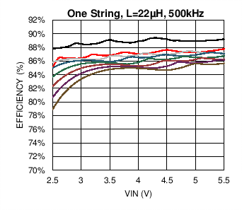
| Top to Bottom: 1x3, 1x4, 1x5, 1x6, 1x7, 1x8, 1x9, 1x10 (LEDs) |
| Top to Bottom: 3x3, 3x4, 3x5, 3x6 (LEDs) |
| Top to Bottom: 2x3, 2x4, 2x5, 2x6, 2x7, 2x8, 2x9, 2x10 (LEDs) |
| Top to Bottom: 1x3, 1x4, 1x5, 1x6, 1x7, 1x8, 1x9, 1x10 (LEDs) |
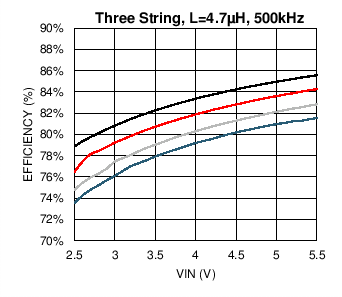
| Top to Bottom: 3x3, 3x4, 3x5, 3x6 (LEDs) |
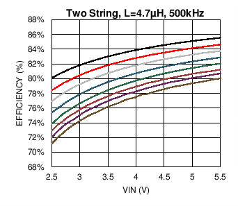
| Top to Bottom: 2x3, 2x4, 2x5, 2x6, 2x7, 2x8, 2x9, 2x10 (LEDs) |
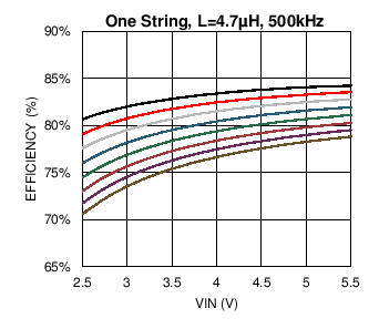
| Top to Bottom: 1x3, 1x4, 1x5, 1x6, 1x7, 1x8, 1x9, 1x10 (LEDs) |
| Top to Bottom: 3x3, 3x4, 3x5, 3x6 (LEDs) |
| Top to Bottom: 2x3, 2x4, 2x5, 2x6, 2x7, 2x8, 2x9, 2x10 (LEDs) |
| Top to Bottom: 3x3, 3x4, 3x5, 3x6 (LEDs) |
| Top to Bottom: 2x3, 2x4, 2x5, 2x6, 2x7, 2x8, 2x9, 2x10 (LEDs) |
| Top to Bottom: 3x3, 3x4, 3x5, 3x6 (LEDs) |
| Top to Bottom: 2x3, 2x4, 2x5, 2x6, 2x7, 2x8, 2x9, 2x10 (LEDs) |
| ILED = 20 mA |
| Exponential Mapping | ||
| Linear Mapping | ||
| Linear Mapping | ||
 Figure 64. LVLED Current vs Current Sink Headroom Voltage
| 50% Duty Cycle |
| 1x Gain |
| 3x6 LEDs |
| Typical Application Circuit | 3 x 6 LEDs | |
| Top to Bottom: 3x3, 3x4, 3x5, 3x6 (LEDs) |
| Top to Bottom: 2x3, 2x4, 2x5, 2x6, 2x7, 2x8, 2x9, 2x10 (LEDs) |
| Top to Bottom: 1x3, 1x4, 1x5, 1x6, 1x7, 1x8, 1x9, 1x10 (LEDs) |
| Top to Bottom: 3x3, 3x4, 3x5, 3x6 (LEDs) |
| Top to Bottom: 2x3, 2x4, 2x5, 2x6, 2x7, 2x8, 2x9, 2x10 (LEDs) |
| Top to Bottom: 1x3, 1x4, 1x5, 1x6, 1x7, 1x8, 1x9, 1x10 (LEDs) |
| Top to Bottom: 3x3, 3x4, 3x5, 3x6 (LEDs) |
| Top to Bottom: 2x3, 2x4, 2x5, 2x6, 2x7, 2x8, 2x9, 2x10 (LEDs) |
| Top to Bottom: 1x3, 1x4, 1x5, 1x6, 1x7, 1x8, 1x9, 1x10 (LEDs) |
| Top to Bottom: 3x3, 3x4, 3x5, 3x6 (LEDs) |
| Top to Bottom: 2x3, 2x4, 2x5, 2x6, 2x7, 2x8, 2x9, 2x10 (LEDs) |
| Top to Bottom: 3x3, 3x4, 3x5, 3x6 (LEDs) |
| Top to Bottom: 2x3, 2x4, 2x5, 2x6, 2x7, 2x8, 2x9, 2x10 (LEDs) |
| Top to Bottom: 3x3, 3x4, 3x5, 3x6 (LEDs) |
| Top to Bottom: 2x3, 2x4, 2x5, 2x6, 2x7, 2x8, 2x9, 2x10 (LEDs) |
| ILED = 20 mA |
| Exponential Mapping | ||
| Exponential Mapping | ||
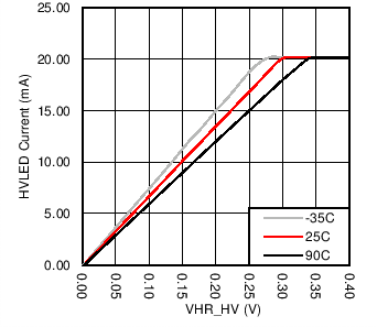
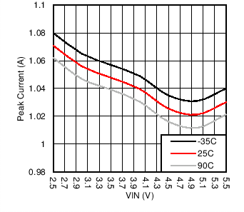 Figure 65. Closed Loop Current Limit vs VIN
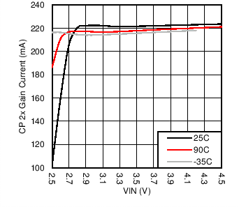
| 2x Gain |
| Pattern Generator Enabled on LVLED1, LVLED2, LVLED3 |
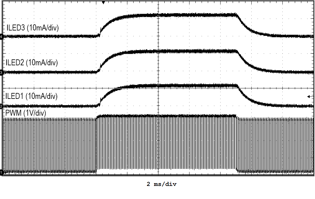
| D = 30% To 90% | ƒPWM = 10 kHz |
8.3 Initialization Set Up
Table 39 shows the minimum number of register writes required for a two-parallel, seven-series LED configuration. This example uses the default settings for ramp times (2048 μsec), mapping mode (exponential) and full-scale current (20.2 mA). In this mode of operation the LM3633 controls the brightness LSBs to ramp between the 8-bit MSB brightness levels providing 11-bit dimming while requiring only 8-bit commands from the host controller.
Table 39. Control Bank A, 8-Bit Control, Two-String, Seven Series LED Configuration Example
| REGISTER NAME | ADDRESS | DATA | DESCRIPTION | |
|---|---|---|---|---|
| HVLED Current Sink Output Configuration | 0x10 | 0x04 | HVLEDs 1 and 2 assigned to Control Bank A | |
| HVLED Current SInk Feedback Enables | 0x28 | 0x03 | Enable feedback on HVLEDs 1 and 2, disable feedback on HVLED 3 | |
| Boost Control | 0x2D | 0x04 | OVP = 32V, ƒsw = 500 kHz | |
| Control Bank Enabled | 0x2B | 0x01 | Enable Control Bank A | |
| Control A Brightness LSB | 0x40 | 0x00 | Control A Brightness LSB written only once | |
| Control A Brightness MSB | 0x41 | User Value | Control A Brightness MSB updated as required | |
Table 40 shows the minimum number of register writes required for a two-parallel, six-series LED configuration with PWM Enabled. This example uses the default settings for ramp times (2048 μsec), mapping mode (exponential) and full-scale current (20.2 mA). In this mode of operation the host controller must update both the brightness LSB and MSB registers whenever a brightness change is required.
Table 40. Control Bank A, 11-Bit Control, Two-String, Six Series LED Configuration Example
| REGISTER NAME | ADDRESS | DATA | DESCRIPTION | |
|---|---|---|---|---|
| HVLED Current Sink Output Configuration | 0x10 | 0x04 | HVLEDs 1 and 2 assigned to Control Bank A | |
| HVLED Current SInk Feedback Enables | 0x28 | 0x03 | Enable feedback on HVLEDs 1 and 2, disable feedback on HVLED 3 | |
| Boost Control | 0x2D | 0x03 | OVP = 24V, ƒsw = 1 MHz | |
| PWM Configuration | 0x2F | 0x0D | PWM Zero Detect = Enabled, PWM Polarity = Active HIgh, Control B PWM = Disabled, Control A PWM = Enabled | |
| Control Bank Enabled | 0x2B | 0x01 | Enable Control Bank A | |
| Control A Brightness LSB | 0x40 | User Value | Control A Brightness LSB written as required (NOTE: The Brightness LSB change does not take effect until the Brightness MSB register is written.) |
|
| Control A Brightness MSB | 0x41 | User Value | Control A Brightness MSB updated as required(1) | |
Table 41 shows the minimum number of register writes required for five low-voltage indicator LEDs. This example uses the default settings for ramp times (2048 μs), mapping mode (exponential) and charge pump and can be combined with either Table 39 or Table 40 above paying careful attention to the Brightness Configuration and Control Bank Enable registers (these registers control both high-voltage and low-voltage LEDs). In this mode of operation the host controller must update both Controls C and F brightness whenever a low-voltage LED brightness change is required. In this example the indicator LEDs is not synchronized due to the time delay between configuration of the Control C and Control F brightness settings. If synchronization of the indicator LED timing is required the user must enable the Control Bank after writing all Control Bank brightness registers.
Table 41. Control Bank A Enable with Control Bank C and Control Bank F Low-Voltage LED Configuration Example
| REGISTER NAME | ADDRESS | DATA | DESCRIPTION | |
|---|---|---|---|---|
| LVLED Current Sink Output Configuration | 0x11 | 0x20 | LVLEDs 1, 2, and 3 assigned to Control Bank C LVLED 4, 5 assigned to Control Bank F, LVLED 6 assigned to Control Bank H |
|
| Control C Full-Scale Current Setting | 0x22 | 0x00 | Set Full-Scale current to 5 mA | |
| Control F Full-Scale Current Setting | 0x25 | 0x00 | Set Full-Scale current to 5 mA | |
| LVLED Current SInk Feedback Enables | 0x29 | 0x1F | Enable feedback on LVLEDs 1, 2, 3, 4, 5; LVLED 6 disabled | |
| Control Bank Enable | 0x2B | 0x25 | Enable LVLED Control Banks F and C with HVLED Control Bank A (If synchronization of indicator LEDs is required enable Control Bank after Control Banks C and F Brightness register configuration) |
|
| Control C Brightness | 0x44 | User Value | Control C Brightness written as required | |
| Control F Brightness | 0x47 | User Value | Control F Brightness updated as required | |
Table 42 shows the minimum number of register writes required to configure the pattern generator for all six low-voltage indicator LEDs. This pattern sequences through all six indicator LEDs using a uniform delay time of 196.608 ms.
Table 42. Low Voltage LED Pattern Generator Configuration Example
| REGISTER NAME | ADDRESS | DATA | DESCRIPTION | |
|---|---|---|---|---|
| LVLED Current Sink Output Configuration | 0x11 | 0x36 | All low-voltage LED current sinks assigned to independent Control Banks | |
| Control C Start-up/Shutdown Ramp Time | 0x14 | 0x33 | Set Start-up and Shutdown Ramp time to 1.049 seconds | |
| Control D Start-up/Shutdown Ramp Time | 0x15 | 0x33 | Set Start-up and Shutdown Ramp time to 1.049 seconds | |
| Control E Start-up/Shutdown Ramp Time | 0x16 | 0x33 | Set Start-up and Shutdown Ramp time to 1.049 seconds | |
| Control F Start-up/Shutdown Ramp Time | 0x17 | 0x33 | Set Start-up and Shutdown Ramp time to 1.049 seconds | |
| Control G Start-up/Shutdown Ramp Time | 0x18 | 0x33 | Set Start-up and Shutdown Ramp time to 1.049 seconds | |
| Control H Start-up/Shutdown Ramp Time | 0x19 | 0x33 | Set Start-up and Shutdown Ramp time to 1.049 seconds | |
| Control C//D/E Ramp Time | 0x1C | 0x33 | Set Ramp Up/Down Transition time to 1.049 seconds | |
| Control F/G/H Ramp Time | 0x1D | 0x33 | Set Ramp Up/Down Transition time to 1.049 seconds | |
| Control C Full-Scale Current Setting | 0x22 | 0x00 | Set Full-Scale current to 5 mA | |
| Control D Full-Scale Current Setting | 0x23 | 0x00 | Set Full-Scale current to 5 mA | |
| Control E Full-Scale Current Setting | 0x24 | 0x00 | Set Full-Scale current to 5 mA | |
| Control F Full-Scale Current Setting | 0x25 | 0x00 | Set Full-Scale current to 5 mA | |
| Control G Full-Scale Current Setting | 0x26 | 0x00 | Set Full-Scale current to 5 mA | |
| Control H Full-Scale Current Setting | 0x27 | 0x00 | Set Full-Scale current to 5 mA | |
| Control C Brightness | 0x44 | 0xA5 | Control C Brightness | |
| Control D Brightness | 0x45 | 0xA5 | Control D Brightness | |
| Control E Brightness | 0x46 | 0xA5 | Control E Brightness | |
| Control F Brightness | 0x47 | 0xA5 | Control F Brightness | |
| Control G Brightness | 0x48 | 0xA5 | Control G Brightness | |
| Control H Brightness | 0x49 | 0xA5 | Control H Brightness | |
| Control C Pattern Generator Delay Time | 0x50 | 0x00 | Set Control C Delay time to 16.384 ms | |
| Control D Pattern Generator Delay Time | 0x60 | 0x0C | Set Control D Delay time to 212.992 ms | |
| Control E Pattern Generator Delay Time | 0x70 | 0x18 | Set Control E Delay time to 409.6 ms | |
| Control F Pattern Generator Delay Time | 0x80 | 0x24 | Set Control F Delay time to 606.208 ms | |
| Control G Pattern Generator Delay Time | 0x90 | 0x30 | Set Control G Delay time to 802.816 ms | |
| Control H Pattern Generator Delay Time | 0xA0 | 0x3C | Set Control H Delay time to 999.424 ms | |
| Control C Pattern Generator Low Time | 0x51 | 0x3A | Set Control C Low Time to 950.27 ms | |
| Control D Pattern Generator Low Time | 0x61 | 0x3A | Set Control D Low Time to 950.27 ms | |
| Control E Pattern Generator Low Time | 0x71 | 0x3A | Set Control E Low Time to 950.27 ms | |
| Control F Pattern Generator Low Time | 0x81 | 0x3A | Set Control F Low Time to 950.27 ms | |
| Control G Pattern Generator Low Time | 0x91 | 0x3A | Set Control G Low Time to 950.27 ms | |
| Control H Pattern Generator Low Time | 0xA1 | 0x3A | Set Control H Low Time to 950.27 ms | |
| Control C Pattern Generator High Time | 0x52 | 0x40 | Set Control C High Time to 1507.33 ms | |
| Control D Pattern Generator High Time | 0x62 | 0x40 | Set Control D High Time to 1507.33 ms | |
| Control E Pattern Generator High Time | 0x72 | 0x40 | Set Control E High Time to 1507.33 ms | |
| Control F Pattern Generator High Time | 0x82 | 0x40 | Set Control F High Time to 1507.33 ms | |
| Control G Pattern Generator High Time | 0x92 | 0x40 | Set Control G High Time to 1507.33 ms | |
| Control H Pattern Generator High Time | 0xA2 | 0x40 | Set Control H High Time to 1507.33 ms | |
| Control C Pattern Generator Low-Level Brightness | 0x53 | 0x01 | Set Control C Low-Level Brightness | |
| Control D Pattern Generator Low-Level Brightness | 0x63 | 0x01 | Set Control D Low-Level Brightness | |
| Control E Pattern Generator Low-Level Brightness | 0x73 | 0x01 | Set Control E Low-Level Brightness | |
| Control F Pattern Generator Low-Level Brightness | 0x83 | 0x01 | Set Control F Low-Level Brightness | |
| Control G Pattern Generator Low-Level Brightness | 0x93 | 0x01 | Set Control G Low-Level Brightness | |
| Control H Pattern Generator Low-Level Brightness | 0xA3 | 0x01 | Set Control H Low-Level Brightness | |
| Pattern Generator Enables | 0x2C | 0xFC | Enable Control Bank C/D/E/F/G/H Pattern Generators | |
| Control Bank Enables | 0x2B | 0xFC | Enable Control Banks C/D/E/F/G/H | |