ZHCSCJ2 June 2014 LM3633
PRODUCTION DATA.
- 1 特性
- 2 应用范围
- 3 说明
- 4 修订历史记录
- 5 Pin Configuration and Functions
- 6 Specifications
-
7 Detailed Description
- 7.1 Overview
- 7.2 Functional Block Diagram
- 7.3 Feature Description
- 7.4
Device Functional Modes
- 7.4.1
High-Voltage LED Control
- 7.4.1.1 High-Voltage Boost Converter
- 7.4.1.2 High-Voltage Current Sinks (HVLED1, HVLED2 and HVLED3)
- 7.4.1.3 High-Voltage Current String Biasing
- 7.4.1.4 Boost Switching-Frequency Select
- 7.4.1.5 Automatic Switching Frequency Shift
- 7.4.1.6 Brightness Register Current Control
- 7.4.1.7 PWM Control
- 7.4.1.8 Start-up/Shutdown Ramp
- 7.4.1.9 Run-Time Ramp
- 7.4.1.10 High-Voltage Control A/B Ramp Select
- 7.4.1.11 LED Current Mapping Modes
- 7.4.1.12 Exponential Mapping
- 7.4.1.13 Linear Mapping
- 7.4.2
Low-Voltage LED Control
- 7.4.2.1 Integrated Charge Pump
- 7.4.2.2 Charge Pump Disabled
- 7.4.2.3 Automatic Gain
- 7.4.2.4 Automatic Gain (Flying Capacitor Detection)
- 7.4.2.5 1X Gain
- 7.4.2.6 2X Gain
- 7.4.2.7 Low-Voltage Current Sinks (LVLED1 to LVLED6)
- 7.4.2.8 Low-Voltage LED Biasing
- 7.4.2.9 Brightness Register Current Control
- 7.4.2.10 LED Current Mapping Modes
- 7.4.2.11 Exponential Mapping
- 7.4.2.12 Linear Mapping
- 7.4.2.13 Start-up/Shutdown Ramp
- 7.4.2.14 Run-Time Ramp
- 7.4.3 Low-Voltage LED Pattern Generator
- 7.4.4 Fault Flags/Protection Features
- 7.4.5 I2C-Compatible Interface
- 7.4.1
High-Voltage LED Control
- 7.5 Register Descriptions
-
8 Applications and Implementation
- 8.1 Application Information
- 8.2
Typical Application
- 8.2.1 Design Requirements
- 8.2.2
Detailed Design Procedure
- 8.2.2.1 Boost Converter Maximum Output Power (Boost)
- 8.2.2.2 Boost Inductor Selection
- 8.2.2.3 Output Capacitor Selection
- 8.2.2.4 Schottky Diode Selection
- 8.2.2.5 Input Capacitor Selection
- 8.2.2.6 Maximum Output Power (Charge Pump)
- 8.2.2.7 Charge Pump Flying Capacitor Selection
- 8.2.2.8 Charge Pump Output Capacitor Selection
- 8.2.2.9 Charge Pump Input Capacitor Selection
- 8.2.3 Application Performance Plots
- 8.3 Initialization Set Up
- 9 Power Supply Recommendations
- 10Layout
- 11器件和文档支持
- 12机械封装和可订购信息
10 Layout
10.1 Layout Guidelines (Boost)
The LM3633 inductive boost converter detects a high switched voltage (up to VOVP) at the SW pin, and a step current (up to ICL_BOOST) through the Schottky diode and output capacitor each switching cycle. The high switching voltage can create interference into nearby nodes due to electric field coupling (I = Cdv/dt). The large step current through the diode and the output capacitor can cause a large voltage spike at the SW pin and the OVP pin due to parasitic inductance in the step current conducting path (V = Ldi/dt). Board layout guidelines are geared towards minimizing this electric field coupling and conducted noise. Figure 73 highlights these two noise-generating components.
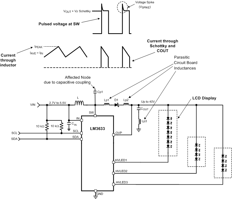 Figure 73. LM3633 Inductive Boost Converter Showing Pulsed Voltage at SW (High dv/dt) and Current Through Schottky and COUT (High di/dt)
The following list details the main (layout sensitive) areas of the LM3633 inductive boost converter in order of decreasing importance:
-
Output Capacitor
- Schottky Cathode to COUT+
- COUT− to GND
-
Schottky Diode
- SW pin to Schottky Anode
- Schottky Cathode to COUT+
-
Inductor
- SW Node PCB capacitance to other traces
-
Input Capacitor
- CIN+ to IN pin
10.1.1 Boost Output Capacitor Placement
Because the output capacitor is in the path of the inductor current discharge path it sees a high-current step from 0 to IPEAK each time the switch turns off and the Schottky diode turns on. Any inductance along this series path from the cathode of the diode through COUT and back into the LM3633 GND pin contributes to voltage spikes (VSPIKE = LP_ × di/dt) at SW and OUT. These spikes can potentially over-voltage the SW pin, or feed through to GND. To avoid this, COUT+ must be connected as close as possible to the Cathode of the Schottky diode, and COUT− must be connected as close as possible to the LM3633 GND bump. The best placement for COUT is on the same layer as the LM3633 so as to avoid any vias that can add excessive series inductance.
10.1.2 Schottky Diode Placement
In the LM3633 boost circuit the Schottky diode is in the path of the inductor current discharge. As a result the Schottky diode sees a high-current step from 0 to IPEAK each time the switch turns off and the diode turns on. Any inductance in series with the diode causes a voltage spike (VSPIKE = LP_ × di/dt) at SW and OUT. This can potentially over-voltage the SW pin, or feed through to VOUT and through the output capacitor and into GND. Connecting the anode of the diode as close as possible to the SW pin and the cathode of the diode as close as possible to COUT+ reduces the inductance (LP_) and minimize these voltage spikes.
10.1.3 Inductor Placement
The node where the inductor connects to the LM3633 SW pin has 2 considerations. First, a large switched voltage (0 to VOUT + VF_SCHOTTKY) appears on this node every switching cycle. This switched voltage can be capacitively coupled into nearby nodes. Second, there is a relatively large current (input current) on the traces connecting the input supply to the inductor and connecting the inductor to the SW pin. Any resistance in this path can cause voltage drops that can negatively affect efficiency and reduce the input operating voltage range.
To reduce the capacitive coupling of the signal on SW into nearby traces, the SW bump-to-inductor connection must be minimized in area. This limits the PCB capacitance from SW to other traces. Additionally, high-impedance nodes that are more susceptible to electric field coupling need to be routed away from SW and not directly adjacent or beneath. This is especially true for traces such as SCL, SDA, HWEN, and PWM. A GND plane placed directly below SW dramatically reduces the capacitance from SW into nearby traces.
Lastly, limit the trace resistance of the VIN-to-inductor connection and from the inductor-to-SW connection, by use of short, wide traces.
10.1.4 Boost Input Capacitor Placement
For the LM3633 boost converter, the input capacitor filters the inductor current ripple, and the internal MOSFET driver currents during turnon of the internal power switch. The driver current requirement can range from 50 mA at 2.7 V to over 200 mA at 5.5 V with fast durations of approximately 10 ns to 20 ns. This appears as high di/dt current pulses coming from the input capacitor each time the switch turns on. Close placement of the input capacitor to the IN pin and to the GND pin is critical since any series inductance between IN and CIN+ or CIN− and GND can create voltage spikes that could appear on the VIN supply line and in the GND plane.
Close placement of the input bypass capacitor at the input side of the inductor is also critical. The source impedance (inductance and resistance) from the input supply, along with the input capacitor of the LM3633, form a series RLC circuit. If the output resistance from the source (RS) is low enough the circuit is underdamped and has a resonant frequency (typically the case). Depending on the size of LS the resonant frequency could occur below, close to, or above the LM3633 switching frequency. This can cause the supply current ripple to be:
- Approximately equal to the inductor current ripple when the resonant frequency occurs well above the LM3633 switching frequency;
- Greater than the inductor current ripple when the resonant frequency occurs near the switching frequency; or
- Less than the inductor current ripple when the resonant frequency occurs well below the switching frequency. Figure 74 shows the series RLC circuit formed from the output impedance of the supply and the input capacitor.
The circuit is redrawn for the AC case where the VIN supply is replaced with a short to GND and the LM3633 + Inductor is replaced with a current source (ΔIL). Equation 1 is the criteria for an underdamped response. Equation 2 is the resonant frequency. Equation 3 is the approximated supply current ripple as a function of LS, RS, and CIN.
As an example, consider a 3.6-V supply with 0.1 Ω of series resistance connected to CIN through 50 nH of connecting traces. This results in an under-damped input-filter circuit with a resonant frequency of 712 kHz. Since both the 1-MHz and 500-kHz switching frequency options lie close to the resonant frequency of the input filter, the supply current ripple is probably larger than the inductor current ripple. In this case, using equation 3, the supply current ripple can be approximated as 1.68 times the inductor current ripple (using a 500 kHz switching frequency) and 0.86 times the inductor current ripple using a 1-MHz switching frequency. Increasing the series inductance (LS) to 500 nH causes the resonant frequency to move to around 225 kHz, and the supply current ripple to be approximately 0.25 times the inductor current ripple (500-kHz switching frequency) and 0.053 times for a 1-MHz switching frequency.
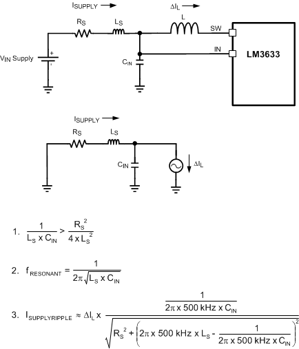 Figure 74. Input RLC Network
10.2 Layout Guidelines (Charge Pump)
The charge pump basically has three areas of concern regarding component placement:
- The flying capacitor (CP)
- The output capacitor (CPOUT)
- The input capacitor
10.2.1 Flying Capacitor (CP) Placement
The charge pump flying capacitor must quickly charge up to the input voltage and then supply the current to the output every switching cycle. Since the charge-pump switching frequency is 1 MHz, the capacitor must be a low-inductance and low-resistive ceramic. Additionally, there must be a low-inductive connection from CP to the LM3633 flying capacitor pin C+ and C−. This is accomplished by placing CP as close as possible to the LM3633 and on the same layer to avoid vias.
10.2.2 Output Capacitor (CPOUT) Placement
The charge pump output capacitor sees the switched charge from the flying capacitor every switching cycle (1 MHz). This fast switching action requires that a low inductive and low resistive capacitor (ceramic) be used and that CPOUT be connected to the LM3633 CPOUT pin with a low inductive connection. This is done by placing CPOUT as close as possible to the CPOUT and GND pins of the LM3633 and on the same layer as the LM3633 to avoid vias.
10.2.3 Charge Pump Input Capacitor Placement
The input capacitor for the LM3633 charge pump is the same one used for the LM3633 inductive boost converter (see Boost Input Capacitor Placement section).
10.3 Layout Example
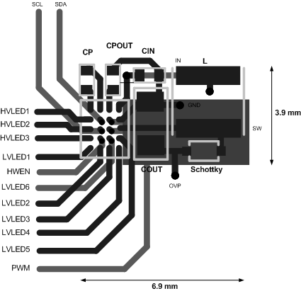 Figure 75. LM3633 Example Layout