ZHCSCJ2 June 2014 LM3633
PRODUCTION DATA.
- 1 特性
- 2 应用范围
- 3 说明
- 4 修订历史记录
- 5 Pin Configuration and Functions
- 6 Specifications
-
7 Detailed Description
- 7.1 Overview
- 7.2 Functional Block Diagram
- 7.3 Feature Description
- 7.4
Device Functional Modes
- 7.4.1
High-Voltage LED Control
- 7.4.1.1 High-Voltage Boost Converter
- 7.4.1.2 High-Voltage Current Sinks (HVLED1, HVLED2 and HVLED3)
- 7.4.1.3 High-Voltage Current String Biasing
- 7.4.1.4 Boost Switching-Frequency Select
- 7.4.1.5 Automatic Switching Frequency Shift
- 7.4.1.6 Brightness Register Current Control
- 7.4.1.7 PWM Control
- 7.4.1.8 Start-up/Shutdown Ramp
- 7.4.1.9 Run-Time Ramp
- 7.4.1.10 High-Voltage Control A/B Ramp Select
- 7.4.1.11 LED Current Mapping Modes
- 7.4.1.12 Exponential Mapping
- 7.4.1.13 Linear Mapping
- 7.4.2
Low-Voltage LED Control
- 7.4.2.1 Integrated Charge Pump
- 7.4.2.2 Charge Pump Disabled
- 7.4.2.3 Automatic Gain
- 7.4.2.4 Automatic Gain (Flying Capacitor Detection)
- 7.4.2.5 1X Gain
- 7.4.2.6 2X Gain
- 7.4.2.7 Low-Voltage Current Sinks (LVLED1 to LVLED6)
- 7.4.2.8 Low-Voltage LED Biasing
- 7.4.2.9 Brightness Register Current Control
- 7.4.2.10 LED Current Mapping Modes
- 7.4.2.11 Exponential Mapping
- 7.4.2.12 Linear Mapping
- 7.4.2.13 Start-up/Shutdown Ramp
- 7.4.2.14 Run-Time Ramp
- 7.4.3 Low-Voltage LED Pattern Generator
- 7.4.4 Fault Flags/Protection Features
- 7.4.5 I2C-Compatible Interface
- 7.4.1
High-Voltage LED Control
- 7.5 Register Descriptions
-
8 Applications and Implementation
- 8.1 Application Information
- 8.2
Typical Application
- 8.2.1 Design Requirements
- 8.2.2
Detailed Design Procedure
- 8.2.2.1 Boost Converter Maximum Output Power (Boost)
- 8.2.2.2 Boost Inductor Selection
- 8.2.2.3 Output Capacitor Selection
- 8.2.2.4 Schottky Diode Selection
- 8.2.2.5 Input Capacitor Selection
- 8.2.2.6 Maximum Output Power (Charge Pump)
- 8.2.2.7 Charge Pump Flying Capacitor Selection
- 8.2.2.8 Charge Pump Output Capacitor Selection
- 8.2.2.9 Charge Pump Input Capacitor Selection
- 8.2.3 Application Performance Plots
- 8.3 Initialization Set Up
- 9 Power Supply Recommendations
- 10Layout
- 11器件和文档支持
- 12机械封装和可订购信息
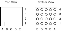
5 Pin Configuration and Functions
DSBGA (YFQ)
20 PINS
Pin Functions
| PIN | DESCRIPTION | |
|---|---|---|
| NAME | NUMBER | |
| C− | A1 | Integrated charge pump flying capacitor negative pin. Connect a 1-µF ceramic capacitor between C+ and C−. |
| C+ | A2 | Integrated charge pump flying capacitor positive pin. Connect a 1-µF ceramic capacitor between C+ and C−. |
| CPOUT | A3 | Integrated charge pump output pin. Bypass CPOUT to GND with a 1-µF ceramic capacitor. |
| IN | A4 | Input voltage connection. Bypass IN to GND with a minimum 2.2-µF ceramic capacitor. |
| HVLED1 | B1 | Input pin to high-voltage current sink 1 (40 V max). The boost converter regulates the minimum of HVLED1, HVLED2 and HVLED3 to VHR. |
| SDA | B2 | Serial data connection for I2C-Compatible Interface. |
| OVP | B3 | Overvoltage sense input. Connect OVP to the positive pin of the inductive boost output capacitor (COUT). |
| GND | B4 | Ground |
| HVLED2 | C1 | Input pin to high-voltage current sink 2 (40 V max). The boost converter regulates the minimum of HVLED1, HVLED2 and HVLED3 to VHR. |
| SCL | C2 | Serial clock connection for I2C-Compatible Interface. |
| PWM | C3 | PWM brightness control input for CABC operation. PWM is a high-impedance input and cannot be left floating. |
| SW | C4 | Drain connection for the internal NFET. Connect SW to the junction of the inductor and the Schottky diode anode. |
| HVLED3 | D1 | Input pin to high-voltage current sink 3 (40 V max). The boost converter regulates the minimum of HVLED1, HVLED2 and HVLED3 to VHR. |
| HWEN | D2 | Hardware enable input. Drive this pin high to enable the device. Drive this pin low to force the device into a low power shutdown. HWEN is a high-impedance input and cannot be left floating. |
| LVLED6 | D3 | Low-voltage current sink 6 |
| LVLED5 | D4 | Low-voltage current sink 5 |
| LVLED1 | E1 | Low-voltage current sink 1 |
| LVLED2 | E2 | Low-voltage current sink 2 |
| LVLED3 | E3 | Low-voltage current sink 3 |
| LVLED4 | E4 | Low-voltage current sink 4 |