ZHCSCJ2 June 2014 LM3633
PRODUCTION DATA.
- 1 特性
- 2 应用范围
- 3 说明
- 4 修订历史记录
- 5 Pin Configuration and Functions
- 6 Specifications
-
7 Detailed Description
- 7.1 Overview
- 7.2 Functional Block Diagram
- 7.3 Feature Description
- 7.4
Device Functional Modes
- 7.4.1
High-Voltage LED Control
- 7.4.1.1 High-Voltage Boost Converter
- 7.4.1.2 High-Voltage Current Sinks (HVLED1, HVLED2 and HVLED3)
- 7.4.1.3 High-Voltage Current String Biasing
- 7.4.1.4 Boost Switching-Frequency Select
- 7.4.1.5 Automatic Switching Frequency Shift
- 7.4.1.6 Brightness Register Current Control
- 7.4.1.7 PWM Control
- 7.4.1.8 Start-up/Shutdown Ramp
- 7.4.1.9 Run-Time Ramp
- 7.4.1.10 High-Voltage Control A/B Ramp Select
- 7.4.1.11 LED Current Mapping Modes
- 7.4.1.12 Exponential Mapping
- 7.4.1.13 Linear Mapping
- 7.4.2
Low-Voltage LED Control
- 7.4.2.1 Integrated Charge Pump
- 7.4.2.2 Charge Pump Disabled
- 7.4.2.3 Automatic Gain
- 7.4.2.4 Automatic Gain (Flying Capacitor Detection)
- 7.4.2.5 1X Gain
- 7.4.2.6 2X Gain
- 7.4.2.7 Low-Voltage Current Sinks (LVLED1 to LVLED6)
- 7.4.2.8 Low-Voltage LED Biasing
- 7.4.2.9 Brightness Register Current Control
- 7.4.2.10 LED Current Mapping Modes
- 7.4.2.11 Exponential Mapping
- 7.4.2.12 Linear Mapping
- 7.4.2.13 Start-up/Shutdown Ramp
- 7.4.2.14 Run-Time Ramp
- 7.4.3 Low-Voltage LED Pattern Generator
- 7.4.4 Fault Flags/Protection Features
- 7.4.5 I2C-Compatible Interface
- 7.4.1
High-Voltage LED Control
- 7.5 Register Descriptions
-
8 Applications and Implementation
- 8.1 Application Information
- 8.2
Typical Application
- 8.2.1 Design Requirements
- 8.2.2
Detailed Design Procedure
- 8.2.2.1 Boost Converter Maximum Output Power (Boost)
- 8.2.2.2 Boost Inductor Selection
- 8.2.2.3 Output Capacitor Selection
- 8.2.2.4 Schottky Diode Selection
- 8.2.2.5 Input Capacitor Selection
- 8.2.2.6 Maximum Output Power (Charge Pump)
- 8.2.2.7 Charge Pump Flying Capacitor Selection
- 8.2.2.8 Charge Pump Output Capacitor Selection
- 8.2.2.9 Charge Pump Input Capacitor Selection
- 8.2.3 Application Performance Plots
- 8.3 Initialization Set Up
- 9 Power Supply Recommendations
- 10Layout
- 11器件和文档支持
- 12机械封装和可订购信息
1 特性
- 驱动三个并联高压发光二极管 (LED) 灯串用于显示和键区照明
- 能够支持高达 40V 输出电压的高压灯串,并且效率高达 90%
- 每个灌电流高达 30mA(背光和指示器)
- 11 位高压 LED 调光
- 针对内容可调亮度控制 (CABC) 的脉宽调制 (PWM) 输入
- 集成型 1A/40V 金属氧化物半导体场效应晶体管 (MOSFET)
- 自适应升压输出至 LED 电压
- 6 个用于指示器 LED 的低压灌电流
- 用来提高效率和 VIN 工作范围的集成电荷泵
- 针对每个指示器 LED 的内部图案生成引擎
- 完全可编程 LED 分组和控制
- 4 个可配置过压保护阀值(16V,24V,32V 和 40V)
- 500kHz 和 1MHz 可编程开关频率
- 过流保护
- 热关断保护
- 27mm2 总体解决方案尺寸
2 应用范围
- 用于智能手机照明的电源
- 显示器、键区和指示器照明
- RGB 指示器驱动器
3 说明
LM3633 11 位 LED 驱动器以高达 90% 的效率为 1,2 或 3 并联高压 LED 灯串提供高性能背光调光功能。 具有集成 1A,40V MOSFET 的升压转换器自动调节至 LED 正向电压,以最大限度地减少净空电压并有效提升 LED 效率。
LM3633 是一款用于智能手机内背光、键区和指示器 LED 的完整电源。 高压电感升压转换器为 3 个并联 LED 灯串(HVLED1,HVLED2 和 HVLED3)供电。 集成电荷泵为 6 个低压指示器 LED (LVLED1-LVLED6) 提供偏置电源。 所有低压灌电流可具有一个可编程图案,此图案可针对多种闪烁图案对他们的输出电流进行调制。
一个额外特性是针对内容可调背光控制的脉宽调制 (PWM) 控制输入,它可被用来控制任一高压灌电流。
LM3633 可由一个 I2C 兼容接口完全可编程。 此器件在 2.7V 至 5.5V 的输入电压范围和 -40°C 至 85°C 的温度范围内运行。
器件信息(1)
| 产品型号 | 封装 | 封装尺寸(最大值) |
|---|---|---|
| LM3633 | 芯片尺寸球状引脚栅格阵列 (DSBGA) (20) | 2.04mm x 1.78mm |
- 要了解所有可用封装,请见数据表末尾的可订购产品附录。
简化电路原理图

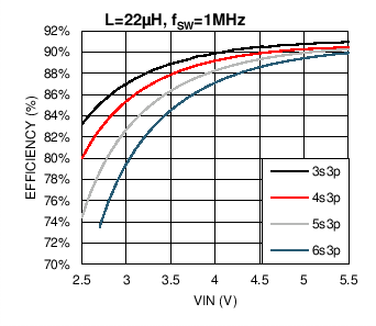
双灯串效率与 VIN 之间的关系