SNOSB43C September 2011 – November 2016 LM3560
PRODUCTION DATA.
- 1 Features
- 2 Applications
- 3 Description
- 4 Revision History
- 5 Pin Configuration and Functions
- 6 Specifications
-
7 Detailed Description
- 7.1 Overview
- 7.2 Functional Block Diagram
- 7.3
Feature Description
- 7.3.1 Power Amplifier Synchronization (Tx1)
- 7.3.2 Independent LED Control
- 7.3.3 Hardware Torch
- 7.3.4 Fault Protections
- 7.3.5 Input Voltage Monitor
- 7.3.6 Last Flash Register
- 7.3.7 LED Voltage Monitor
- 7.3.8 ADC Delay
- 7.3.9 Flags Register and Fault Indicators
- 7.4
Device Functional Modes
- 7.4.1 Start-Up (Enabling the Device)
- 7.4.2 Pass Mode
- 7.4.3 Flash Mode
- 7.4.4 Torch Mode
- 7.4.5 Privacy Indicator Mode
- 7.4.6 GPIO1 Mode
- 7.4.7 TX2/INT/GPIO2
- 7.4.8 TX2 Mode
- 7.4.9 GPIO2 Mode
- 7.4.10 Interrupt Output (INT Mode)
- 7.4.11 NTC Mode
- 7.4.12 Alternate External Torch (AET) Mode
- 7.4.13 Automatic Conversion Mode
- 7.4.14 Manual Conversion Mode
- 7.5 I2C-Compatible Interface
- 7.6
Register Descriptions
- 7.6.1 Enable Register (Address 0x10)
- 7.6.2 Privacy Register (Address 0x11)
- 7.6.3 Indicator Register (Address 0x12)
- 7.6.4 Indicator Blinking Register (Address 0x13)
- 7.6.5 Privacy PWM Period Register (Address 0x14)
- 7.6.6 GPIO Register (Address 0x20)
- 7.6.7 LED Forward Voltage ADC (VLED Monitor Register, Address 0x30)
- 7.6.8 ADC Delay Register (Address 0x31)
- 7.6.9 VIN Monitor Register (Address 0x80)
- 7.6.10 Last Flash Register (Address 0x81)
- 7.6.11 Torch Brightness Register Descriptions (Address 0xA0)
- 7.6.12 Flash Brightness Register (Address 0xB0)
- 7.6.13 Flash Duration Register (Address 0xC0)
- 7.6.14 Flags Register (Address 0xD0)
- 7.6.15 Configuration Register 1 (Address 0xE0)
- 7.6.16 Configuration Register 2 (Address 0xF0)
- 8 Application and Implementation
- 9 Power Supply Recommendations
- 10Layout
- 11Device and Documentation Support
- 12Mechanical, Packaging, and Orderable Information
6 Specifications
6.1 Absolute Maximum Ratings
over operating free-air temperature range (unless otherwise noted)(1)| MIN | MAX | UNIT | ||
|---|---|---|---|---|
| VIN, VSW, VOUT | –0.3 | 6 | V | |
| VSCL, VSDA, VHWEN, VSTROBE, VTX1, VTX2, VLED1, VLED2, VLEDI/NTC | –0.3 | to the lesser of (VIN + 0.3 V) with 6 V maximum | V | |
| Continuous power dissipation(2) | Internally limited | |||
| Junction temperature, TJ-MAX | 150 | °C | ||
| Storage temperature, Tstg | –65 | 150 | °C | |
(1) Stresses beyond those listed under Absolute Maximum Ratings may cause permanent damage to the device. These are stress ratings only, which do not imply functional operation of the device at these or any other conditions beyond those indicated under Recommended Operating Conditions. Exposure to absolute-maximum-rated conditions for extended periods may affect device reliability.
6.2 ESD Ratings
| VALUE | UNIT | |||
|---|---|---|---|---|
| V(ESD) | Electrostatic discharge | Human-body model (HBM), per ANSI/ESDA/JEDEC JS-001(1) | ±2000 | V |
(1) JEDEC document JEP155 states that 500-V HBM allows safe manufacturing with a standard ESD control process.
6.3 Recommended Operating Conditions
over operating free-air temperature range (unless otherwise noted)| MIN | MAX | UNIT | ||
|---|---|---|---|---|
| Input voltage, VIN | 2.5 | 5.5 | V | |
| Junction temperature, TJ | –40 | 125 | °C | |
| Ambient temperature, TA(1) | –40 | 85 | °C | |
(1) In applications where high power dissipation and/or poor package thermal resistance is present, the maximum ambient temperature may have to be derated. Maximum ambient temperature (TA-MAX) is dependent on the maximum operating junction temperature (TJ-MAX-OP = 125°C), the maximum power dissipation of the device in the application (PD-MAX), and the junction-to-ambient thermal resistance of the device package in the application (RθJA), as given by the following equation: TA-MAX = TJ-MAX-OP – (RθJA × PD-MAX).
6.4 Thermal Information
| THERMAL METRIC(1) | LM3560 | UNIT | |
|---|---|---|---|
| YZR (DSBGA) | |||
| 16 PINS | |||
| RθJA | Junction-to-ambient thermal resistance | 71.4 | °C/W |
| RθJC(top) | Junction-to-case (top) thermal resistance | 0.4 | °C/W |
| RθJB | Junction-to-board thermal resistance | 12.4 | °C/W |
| ψJT | Junction-to-top characterization parameter | 0.3 | °C/W |
| ψJB | Junction-to-board characterization parameter | 12.6 | °C/W |
(1) For more information about traditional and new thermal metrics, see Semiconductor and IC Package Thermal Metrics.
6.5 Electrical Characteristics
Unless otherwise specified, VIN = 3.6 V, VHWEN = VIN, TA = 25°C.(1) (2)| PARAMETER | TEST CONDITIONS | MIN | TYP | MAX | UNIT | |||
|---|---|---|---|---|---|---|---|---|
| CURRENT SOURCE SPECIFICATIONS | ||||||||
| ILED | Current source accuracy | ILED1 + ILED2
3 V ≤ VIN ≤ 4.2 V VOUT = 4.5 V |
1000-mA flash current setting, per current source | –3.5% | 2000 | 3.5% | mA | |
| 1000-mA flash current setting, per current source –40°C ≤ TA ≤ 85°C |
–5% | 5% | ||||||
| 31.25-mA torch current, per current source | 62.5 | |||||||
| 31.25-mA torch current, per current source –40°C ≤ TA ≤ 85°C |
–10% | 10% | ||||||
| VOUT – VLED1/2 | Current source regulation voltage | ILED = 2 A (ILED1 + ILED2), VOUT = 4.5 V | 300 | mV | ||||
| VOVP | Output overvoltage protection trip point(3) | ON threshold | 5 | V | ||||
| ON threshold, –40°C ≤ TA ≤ 85°C | 4.925 | 5.075 | ||||||
| OFF threshold | 4.8 | |||||||
| STEP-UP DC-DC CONVERTER SPECIFICATIONS | ||||||||
| RPMOS | PMOS switch on-resistance | IPMOS = 1 A | 80 | mΩ | ||||
| RNMOS | NMOS switch on-resistance | INMOS = 1 A | 65 | mΩ | ||||
| ICL | Switch current limit(4) | CL bits = 00 | 1.6 | A | ||||
| CL bits = 00, 3 V ≤ VIN ≤ 4.2 V –40°C ≤ TA ≤ 85°C |
1.44 | 1.76 | ||||||
| CL bits = 01 | 2.3 | |||||||
| CL bits = 01, 3 V ≤ VIN ≤ 4.2 V –40°C ≤ TA ≤ 85°C |
2.02 | 2.58 | ||||||
| CL bits = 10 | 3 | |||||||
| CL bits = 10, 3 V ≤ VIN ≤ 4.2 V –40°C ≤ TA ≤ 85°C |
2.64 | 3.36 | ||||||
| CL bits = 11 | 3.6 | |||||||
| CL bits = 11, 3 V ≤ VIN ≤ 4.2 V –40°C ≤ TA ≤ 85°C |
3.17 | 4.03 | ||||||
| IOUT_SC | Output short-circuit current limit | VOUT < 2.3 V | 300 | mA | ||||
| ILEDI/NTC | Indicator current | Message indicator register, bits[2:0] = 111 VLEDI/NTC = 2 V |
18 | mA | ||||
| Message indicator register, bits[2:0] = 111, 3 V ≤ VIN ≤ 4.2 V VLEDI/NTC = 2 V, –40°C ≤ TA ≤ 85°C |
16 | 20 | ||||||
| VTRIP | Comparator trip threshold | Configuration register 1, bit [4] = 1, | 1 | V | ||||
| Configuration register 1, bit [4] = 1, 3 V ≤ VIN ≤ 4.2 V, –40°C ≤ TA ≤ 85°C |
0.97 | 1.03 | ||||||
| ƒSW | Switching frequency | 2 | MHz | |||||
| 3 V ≤ VIN ≤ 4.2 V, –40°C ≤ TA ≤ 85°C | 1.8 | 2.2 | ||||||
| tTIMEOUT | Timeout duration(5)(6) | 3 V ≤ VIN ≤ 4.2 V | –10% | 10% | ms | |||
| IQ | Quiescent supply current | Device not switching, VOUT = 3 V | 900 | µA | ||||
| Device switching, VOUT = 4.5 V | 1.97 | mA | ||||||
| Indicate mode, message indicator register bits [2:0] = 111 | 590 | µA | ||||||
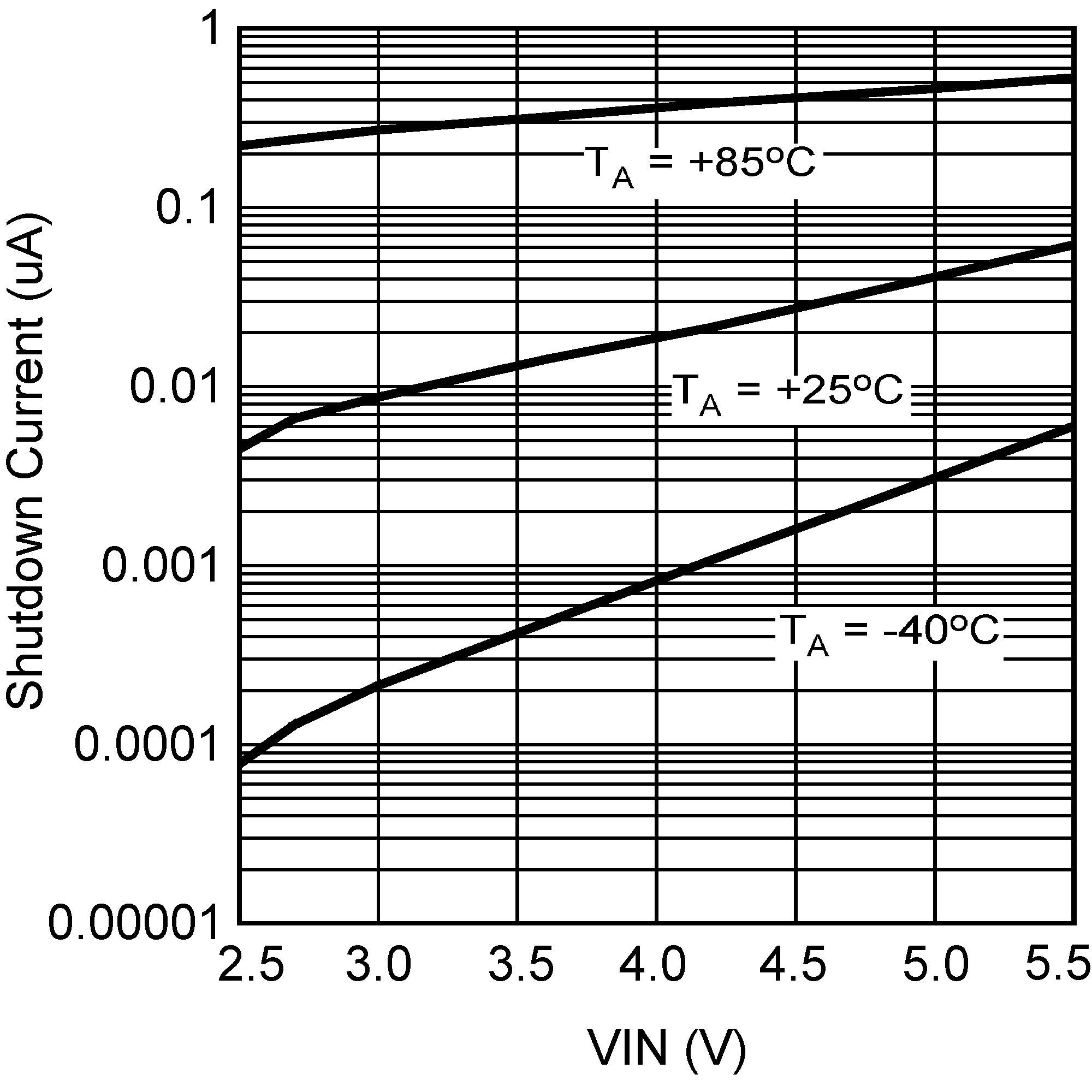
| ISHDN | Shutdown supply current | 3 V ≤ VIN ≤ 4.2 V | 0.02 | µA | ||||
| 3 V ≤ VIN ≤ 4.2 V, –40°C ≤ TA ≤ 85°C | 1.25 | |||||||
| ISTBY | Standby supply current | 1.25 | µA | |||||
| 3 V ≤ VIN ≤ 4.2 V, –40°C ≤ TA ≤ 85°C | 2 | |||||||
| VIN_TH | VIN monitor threshold | VIN monitor register = 0x01 | 2.9 | V | ||||
| VIN monitor register = 0x01, –40°C ≤ TA ≤ 85°C | 2.85 | 2.95 | ||||||
| VIN_FLASH_TH | VIN flash monitor threshold | VIN monitor register = 0x08 | 2.9 | V | ||||
| VIN monitor register = 0x08, –40°C ≤ TA ≤ 85°C | 2.85 | 2.95 | ||||||
| tTX | Flash-to-torch LED current settling time | TX_ Low to high ILED1 + ILED2 = 2 A to 187.5 mA |
2 | µs | ||||
| Torch-to-flash LED current Settling | TX_High to low ILED1 + ILED2 = 187.5 mA to 2 mA |
160 | ||||||
| tD | Time from when ILED hits target until VLED data is available | ADC delay register bit [5] = 1 | 16 | µs | ||||
| ADC delay register bit [5] = 0 ADC delay register bits [4:0] = 0000 |
250 | |||||||
| VF_ADC | ADC threshold | VLED monitor register bits [3:0] = 1111 | 4.2 | V | ||||
| VLED monitor register bits [3:0] = 1111 3 V ≤ VIN ≤ 4.2 V, –40°C ≤ TA ≤ 85°C |
4.05 | 4.35 | ||||||
| HWEN, STROBE, TX1/TORCH/GPIO1, TX2/INT/GPIO2 VOLTAGE SPECIFICATIONS | ||||||||
| VIL | Input logic low | 2.7 V ≤ VIN ≤ 4.2 V, –40°C ≤ TA ≤ 85°C | 0 | 0.4 | V | |||
| VIH | Input logic high | 2.7 V ≤ VIN ≤ 4.2 V, –40°C ≤ TA ≤ 85°C | 1.2 | VIN | V | |||
| RPD | Internal pulldown resistance on TX1, TX2, STROBE | 300 | kΩ | |||||
| I2C-COMPATIBLE VOLTAGE SPECIFICATIONS (SCL, SDA) | ||||||||
| VIL | Input logic low | 2.7 V ≤ VIN ≤ 4.2 V, –40°C ≤ TA ≤ 85°C | 0 | 0.4 | V | |||
| VIH | Input logic high | 2.7 V ≤ VIN ≤ 4.2 V, –40°C ≤ TA ≤ 85°C | 1.3 | VIN | V | |||
| VOL | Output logic low (SDA) | ILOAD = 3 mA 2.7 V ≤ VIN ≤ 4.2 V, –40°C ≤ TA ≤ 85°C |
0.4 | V | ||||
(1) All voltages are with respect to the potential at the GND pin.
(2) Minimum (MIN) and maximum (MAX) limits are specified by design, test, or statistical analysis. Typical (TYP) numbers represent the most likely norm. Unless otherwise stated, conditions for typical specifications are: VIN = 3.6 V and TA = 25°C.
(3) The typical curve for overvoltage protection (OVP) is measured in closed loop using Figure 41 . The OVP value is found by forcing an open circuit in the LED1 and LED2 path and recording the peak value of VOUT. The value given in Electrical Characteristics is found in an open loop configuration by ramping the voltage at OUT until the OVP comparator trips. The closed loop data can appear higher due to the stored energy in the inductor being dumped into the output capacitor after the OVP comparator trips. Worst case is an open circuit condition where the output voltage can continue to rise after the OVP comparator trips by approximately IIN × sqrt(L/COUT).
(4) The typical curve for current limit is measured in closed loop using Figure 41, and increasing IOUT until the peak inductor current stops increasing. The value given in Electrical Characteristics is measured open loop and is found by forcing current into SW until the current limit comparator threshold is reached. Closed loop data appears higher due to the delay between the comparator trip point and the NFET turning off. This delay allows the closed loop inductor current to ramp higher after the trip point by approximately 20 ns × VIN/L.
(5) Specified by design. Not production tested.
(6) The timeout period is a divided down representation of the 2-MHz clock; thus, the accuracy specification is the same as the switching frequency.
6.6 I2C Timing Specifications (SCL, SDA)
All minimum and maximum values apply over –40°C ≤ TA ≤ 85°C and are specified by design (not production tested); see(1)| MIN | MAX | UNIT | ||
|---|---|---|---|---|
| ƒSCL | SCL (clock frequency) | 0 | 400 | kHz |
| tRISE | Rise time of both SDA and SCL | 20 ns + 0.1 × CBUS | 300 | ns |
| tFALL | Fall time of both SDA and SCL | 20 ns + 0.1 × CBUS | 300 | ns |
| tLOW | Low period of SCL clock | 1.3 | µs | |
| tHIGH | High period of SCL clock | 600 | ns | |
| tHD;STA | Hold time for start (or repeated start) condition | 600 | ns | |
| tSU:STA | Set-up time for a repeated start | 600 | ns | |
| tHD:DAT | Data hold time | 0 | ns | |
| tSU:DAT | Data set-up time | 100 | ns | |
| tSU:STO | Set-up time for stop condition | 600 | ns | |
| tVD:DAT | Data valid time | 900 | ns | |
| tVD;ACK | Data valid acknowledge time | 900 | ns | |
| tBUF | Bus-free time between a start and stop condition | 1.3 | µs | |
(1) Specified by design, not production tested.
6.7 Typical Characteristics
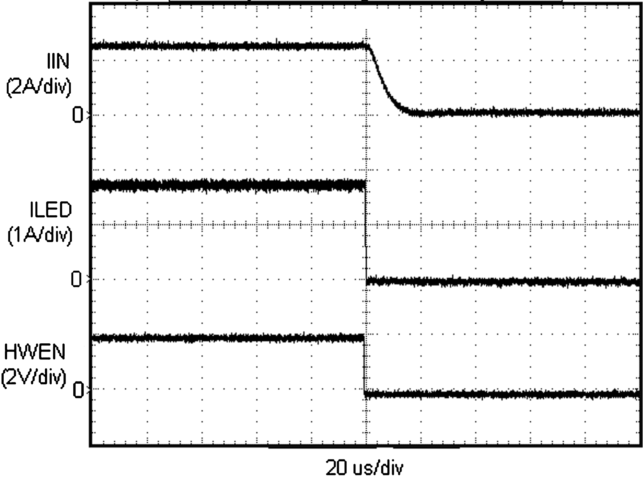
VIN = 3.6 V, COUT = 10 µF, CIN = 10 µF, L = 1 µH (TOKO FDSD0312-1R0, RL = 43 mΩ), TA = 25°C, ILED = ILED1 + ILED2, unless otherwise noted.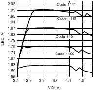
| Highest 4 Flash Brightness Codes | ||
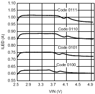
| Lower Middle 4 Flash Brightness Codes | ||
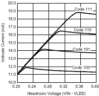
| VLED = 2.5 V | Indicate Codes 100 - 111 |
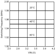
| HWEN = GND |
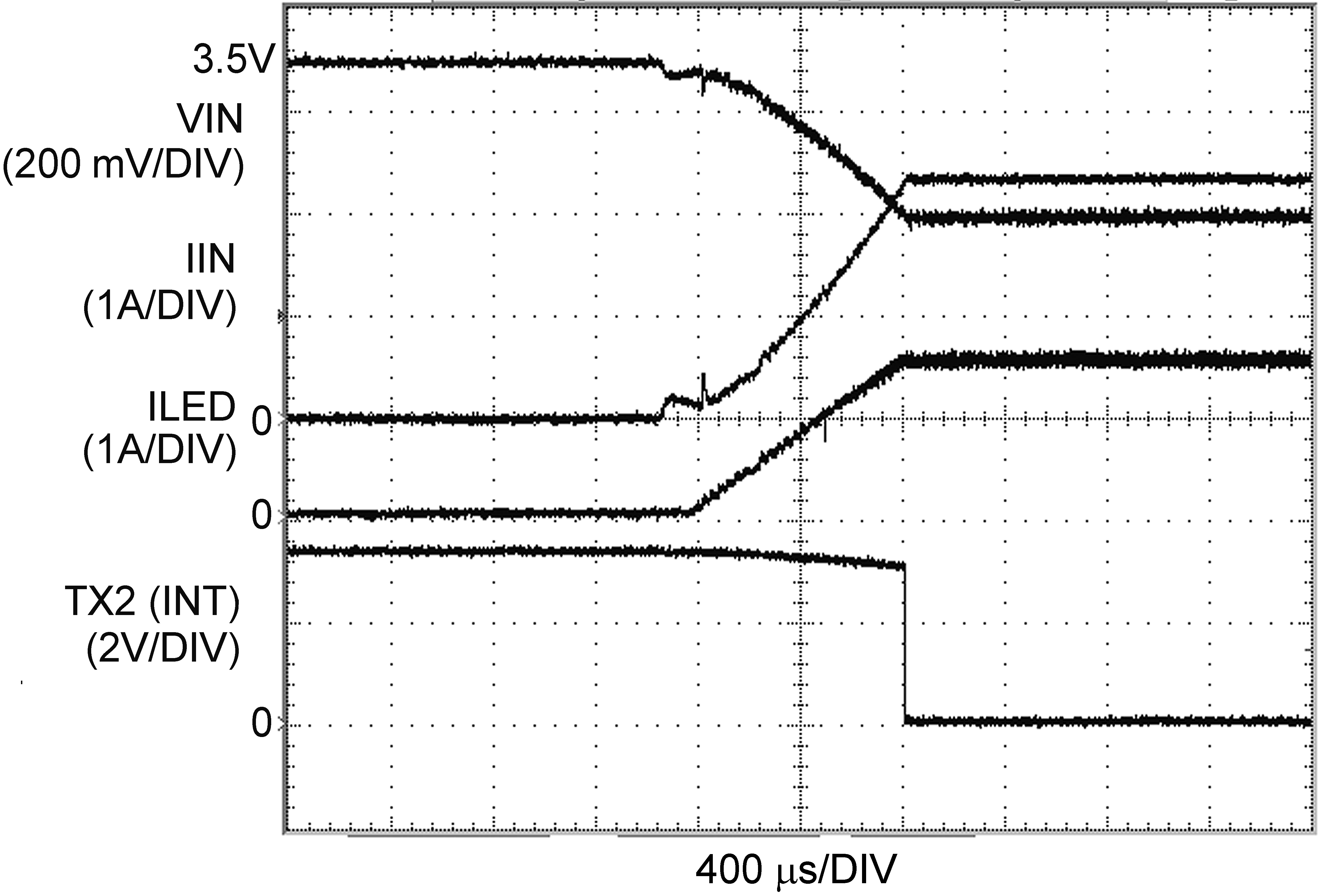
| VIN_FLASH_TH = 3.2 V | TX2 Set For Interrupt Output (INT) | |
| Circuit Of Figure 27 (Note 1) | ||
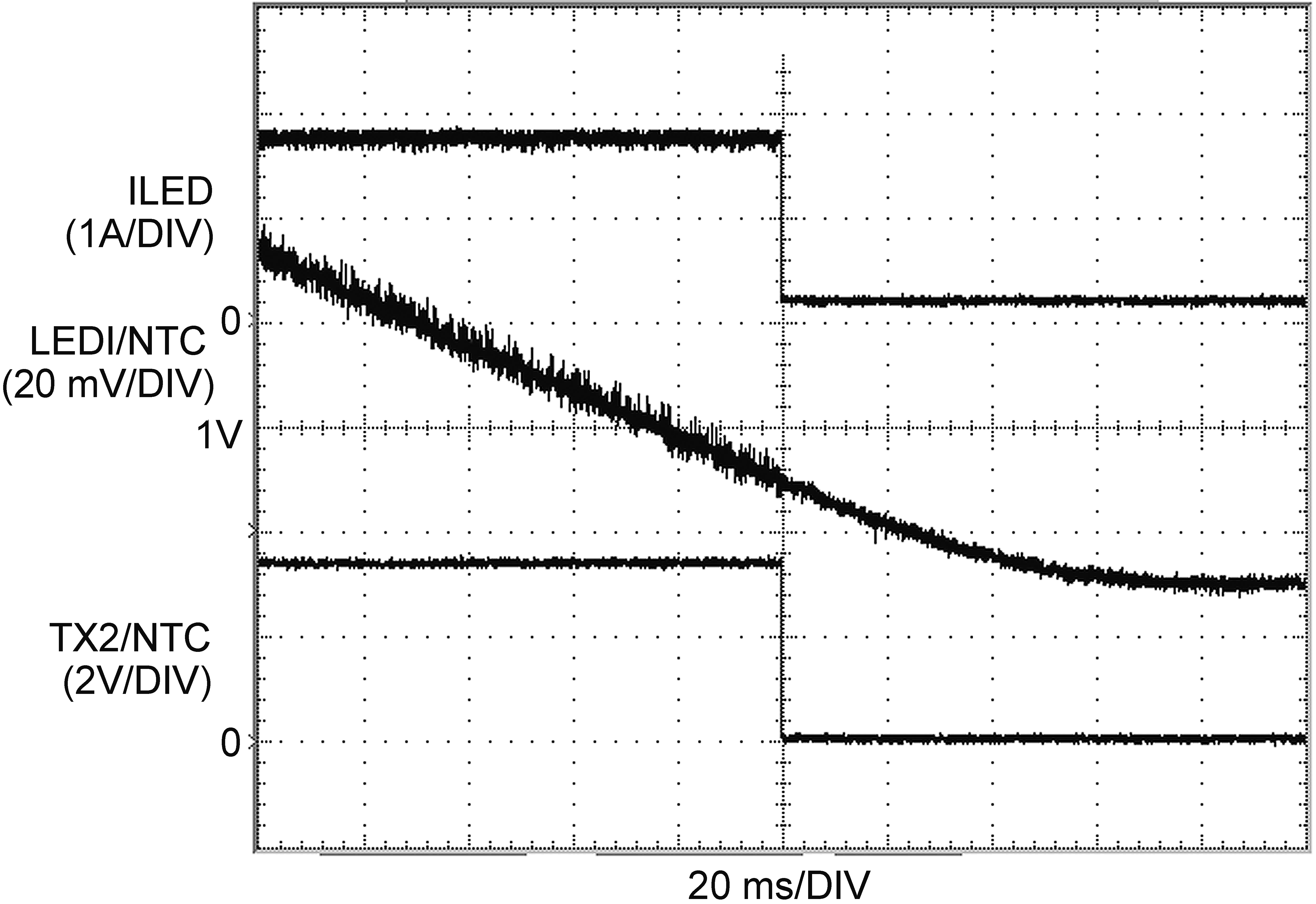
| TX2 Set for Interrupt Output (INT) | R3 = 1.3 kΩ | |
| Circuit of Figure 42 | RNTC = 10 kΩ at 25°C | |
| NTC Set to Force Torch Mode | Beta = 3380 k | |
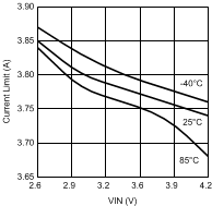
| 3.6-A Setting | See Note 1 |
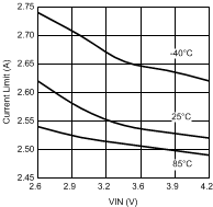
| 2.3-A Setting | See Note 2 |
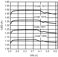
| Upper Middle 4 Flash Brightness Codes | ||
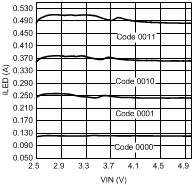
| Lowest 4 Flash Brightness Codes | ||
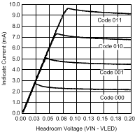
| VLED = 2.5 V | Indicate Codes 000 - 011 |
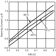
| HWEN = VIN |
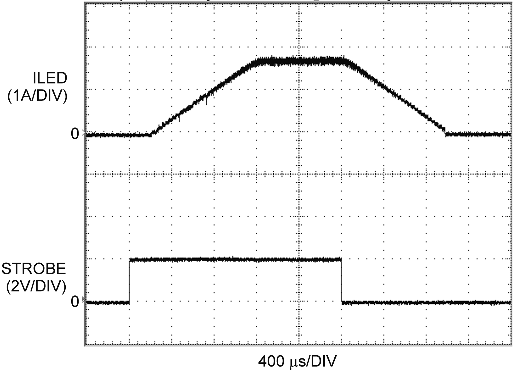
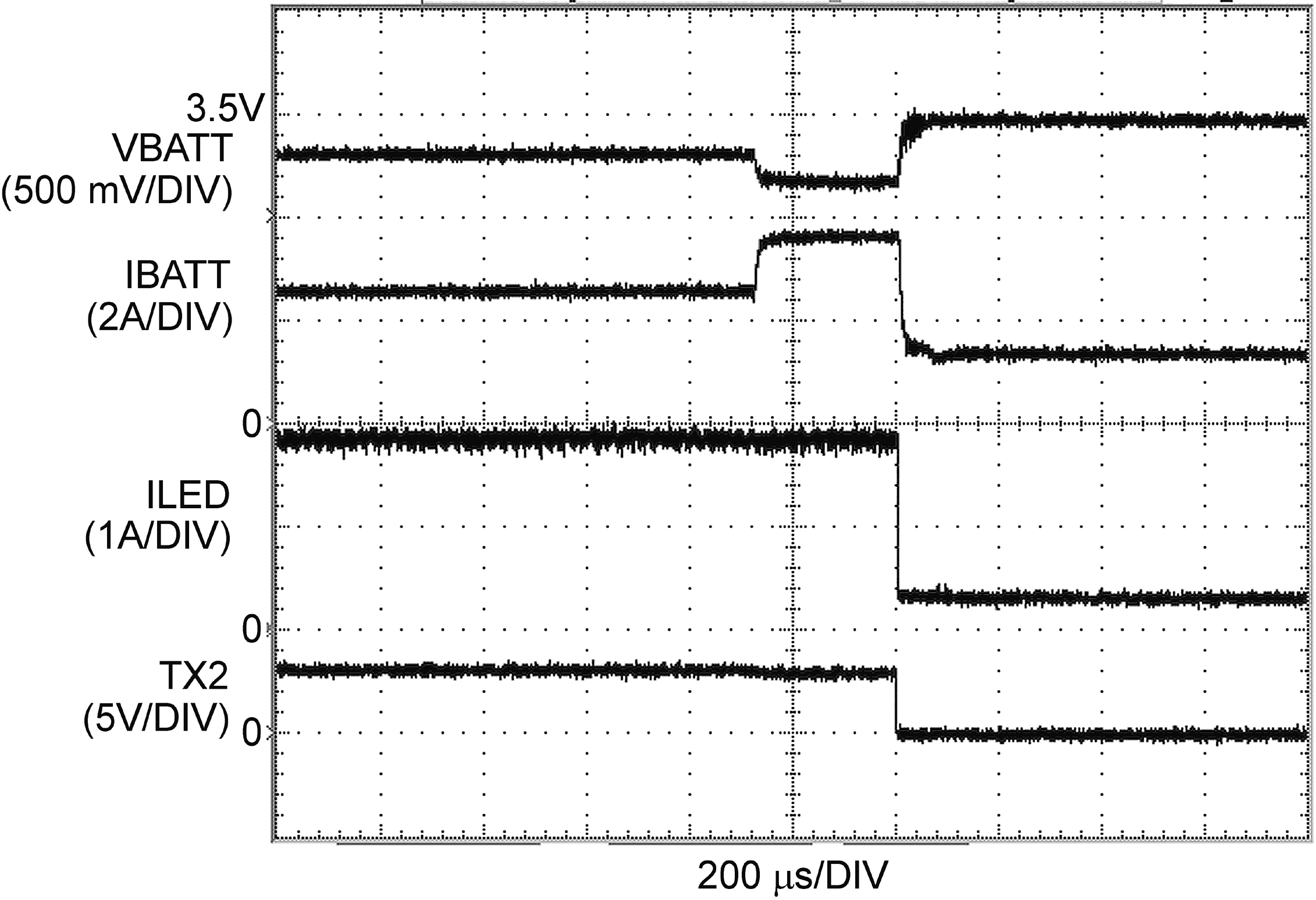
| VIN_TH = 3.2 V | TX2 Set For Interrupt Output (INT) | |
| Circuit of Figure 27 (Note 2) | Force Torch Mode | |
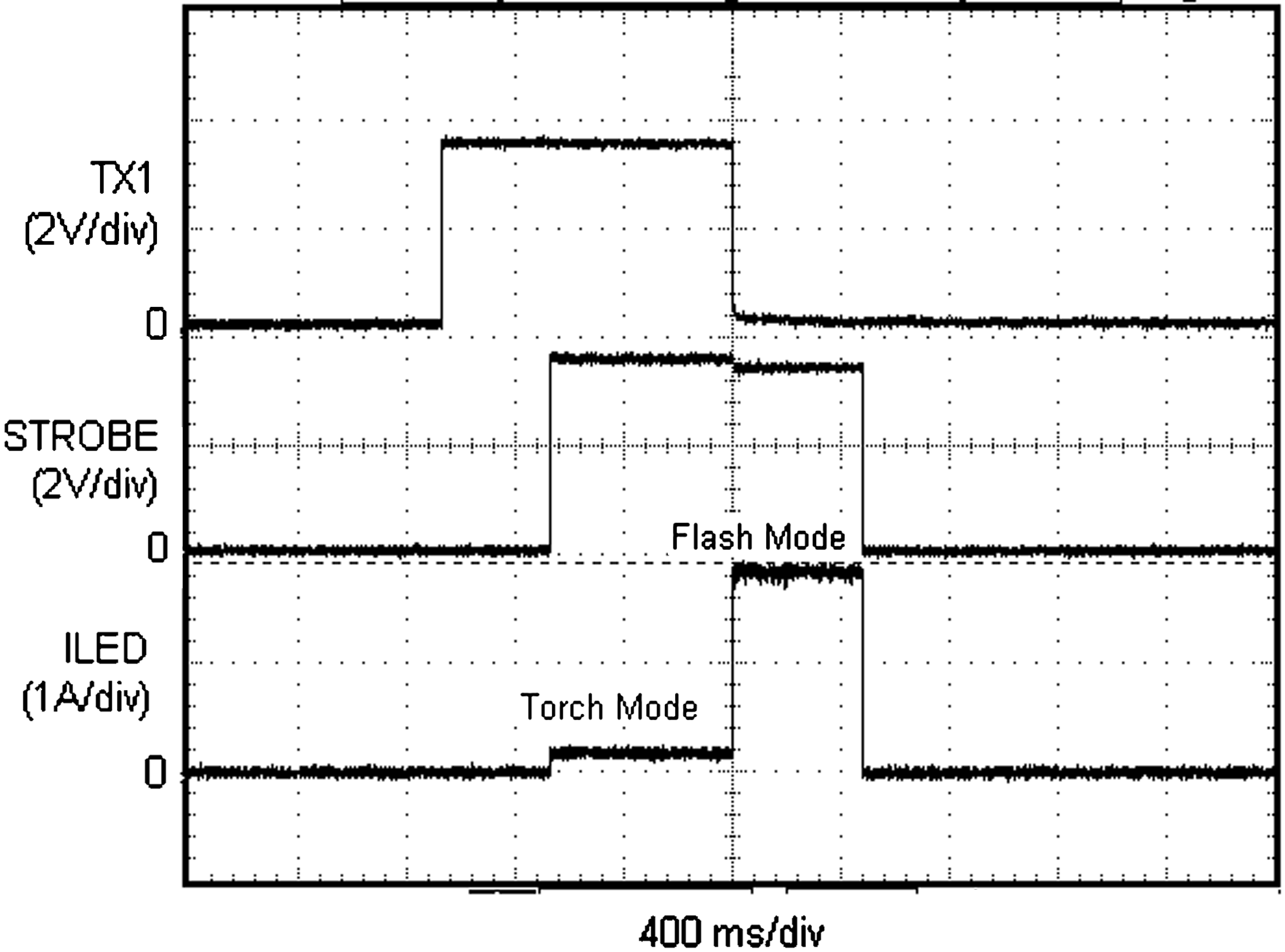
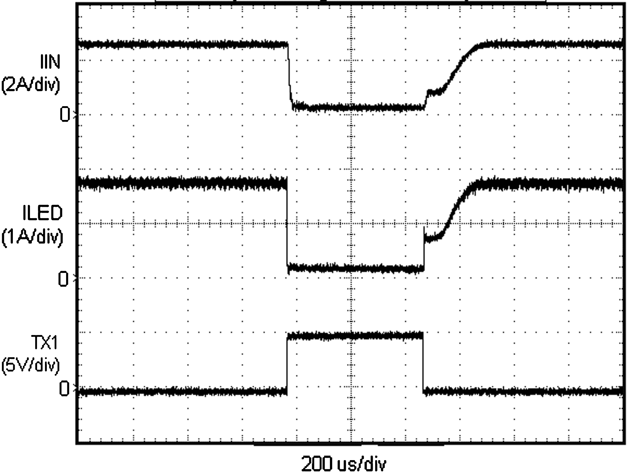
| Force Torch |
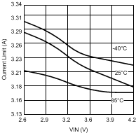
| 3-A Setting | See Note 1 |
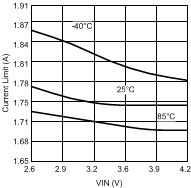
| 1.6-A Setting | See Note 2 |
|
1. The typical curve for current limit is measured in closed loop using Figure 41, and increasing IOUT until the peak inductor current stops increasing. The value given in Electrical Characteristics is measured open loop and is found by forcing current into SW until the current limit comparator threshold is reached. Closed loop data appears higher due to the delay between the comparator trip point and the NFET turning off. This delay allows the closed loop inductor current to ramp higher after the trip point by approximately 20 ns × VIN/L.
|
||
|
1. The typical curve for overvoltage protection (OVP) is measured in closed loop using Figure 41 . The OVP value is found by forcing an open circuit in the LED1 and LED2 path and recording the peak value of VOUT. The value given in Electrical Characteristics is found in an open loop configuration by ramping the voltage at OUT until the OVP comparator trips. The closed loop data can appear higher due to the stored energy in the inductor being dumped into the output capacitor after the OVP comparator trips. Worst case is an open circuit condition where the output voltage can continue to rise after the OVP comparator trips by approximately IIN × sqrt(L/COUT).
|