SNVS569C May   2009  – October 2016 LM3550

PRODUCTION DATA.  

  1. Features
  2. Applications
  3. Description
  4. Revision History
  5. Pin Configuration and Functions
  6. Specifications
    1. 6.1 Absolute Maximum Ratings
    2. 6.2 ESD Ratings
    3. 6.3 Recommended Operating Conditions
    4. 6.4 Thermal Information
    5. 6.5 Electrical Characteristics
    6. 6.6 Timing Requirements
    7. 6.7 Typical Characteristics
  7. Detailed Description
    1. 7.1 Overview
    2. 7.2 Functional Block Diagram
    3. 7.3 Feature Description
      1. 7.3.1 STROBE Pin
      2. 7.3.2 End-of-Charge Pin (EOC)
      3. 7.3.3 ALD/TEMP Pin
      4. 7.3.4 IND Pin
      5. 7.3.5 BAL Pin
      6. 7.3.6 Super-Capacitor Charging Time
      7. 7.3.7 Super-Capacitor Voltage Profile
      8. 7.3.8 Peak Flash Current
      9. 7.3.9 Maximum Flash Duration
    4. 7.4 Device Functional Modes
      1. 7.4.1 State Machine Description
        1. 7.4.1.1 Basic Description
        2. 7.4.1.2 Shutdown State
        3. 7.4.1.3 Torch State
        4. 7.4.1.4 Charge State
          1. 7.4.1.4.1 Fixed-Voltage-Charge Mode
          2. 7.4.1.4.2 Optimal Charge Mode
        5. 7.4.1.5 Torch and Charge State
        6. 7.4.1.6 Flash State
        7. 7.4.1.7 EOC Functionality
        8. 7.4.1.8 State Diagram FGATE = 1
        9. 7.4.1.9 Optimal Charge Mode vs Fixed Voltage Mode
          1. 7.4.1.9.1 Optimal Charge Mode vs Fixed Voltage Mode
    5. 7.5 Programming
      1. 7.5.1 I2C-Compatible Interface
        1. 7.5.1.1 Data Validity
        2. 7.5.1.2 Start and Stop Conditions
        3. 7.5.1.3 Transferring Data
        4. 7.5.1.4 I2C-Compatible Child Address: 0x53
    6. 7.6 Register Maps
      1. 7.6.1 Internal Registers
        1. 7.6.1.1 General Purpose Register Description
        2. 7.6.1.2 Current Control Register Description
        3. 7.6.1.3 Options Control Register Description
        4. 7.6.1.4 ALD/TEMP Sense High/Low Registers
  8. Application and Implementation
    1. 8.1 Application Information
    2. 8.2 Typical Application
      1. 8.2.1 Design Requirements
      2. 8.2.2 Detailed Design Procedure
        1. 8.2.2.1 Component Selection
          1. 8.2.2.1.1 Super-Capacitor
          2. 8.2.2.1.2 Boost Capacitors
          3. 8.2.2.1.3 Current Source FET
          4. 8.2.2.1.4 ALD/TEMP Components
            1. 8.2.2.1.4.1 NTC Selection
            2. 8.2.2.1.4.2 Ambient Light Sensor
          5. 8.2.2.1.5 Thermal Protection
      3. 8.2.3 Application Curves
  9. Power Supply Recommendations
  10. 10Layout
    1. 10.1 Layout Guidelines
    2. 10.2 Layout Example
  11. 11Device and Documentation Support
    1. 11.1 Device Support
      1. 11.1.1 Third-Party Products Disclaimer
      2. 11.1.2 Device Nomenclature
    2. 11.2 Related Documentation
    3. 11.3 Receiving Notification of Documentation Updates
    4. 11.4 Community Resources
    5. 11.5 Trademarks
    6. 11.6 Electrostatic Discharge Caution
    7. 11.7 Glossary
  12. 12Mechanical, Packaging, and Orderable Information

封装选项

机械数据 (封装 | 引脚)
散热焊盘机械数据 (封装 | 引脚)
订购信息

10 Layout

10.1 Layout Guidelines

The UQFN is a leadless package with very good thermal properties. This package has an exposed DAP (die attach pad) at the underside center of the package measuring 1.86 mm × 2.2 mm. The main advantage of this exposed DAP is to offer low thermal resistance when soldered to the thermal ground pad on the PCB. For good PCB layout TI recommends a 1:1 ratio between the package and the PCB thermal land. To further enhance thermal conductivity, the PCB thermal ground pad may include vias to a 2nd layer ground plane. For more detailed instructions on mounting UQFN packages, refer to AN-1187 Leadless Leadframe Package (LLP).

The proceeding steps must be followed to ensure stable operation and proper current source regulation.

  1. Bypass VIN with at least a 4.7-µF ceramic capacitor. Connect the positive terminal of this capacitor as close as possible to VIN.
  2. Connect COUT as close as possible to the VOUT pin with at least a 2.2-µF capacitor.
  3. Connect the return terminals of the input capacitor and the output capacitor as close as possible to the exposed DAP and GND pins through low impedance traces.
  4. Place the two 1-µF flying capacitors (C1 and C2) as close as possible to the LM3550 C1+, C1− and C2+, C2− pins.
  5. To minimize losses during the flash pulse, TI recommends that the flash LEDs, the current source NFET, and current-setting resistor be placed as close as possible to the super capacitor.

10.2 Layout Example
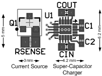
LM3550 30059459.gif Figure 72. LM3550 Layout